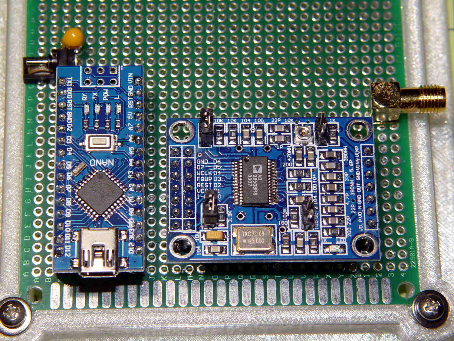
Compare this picture:
… with any of the doc for the generic AD8950/51 DDS modules you’ll find out on the Interwebs. This snippet from the seller’s schematic will suffice:
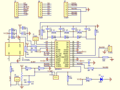
Here’s a closer look at the 2×7 header in the upper left corner:
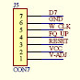
Don’t blame me for the blur, the schematic is a JPG.
Compared it with the board in hand:
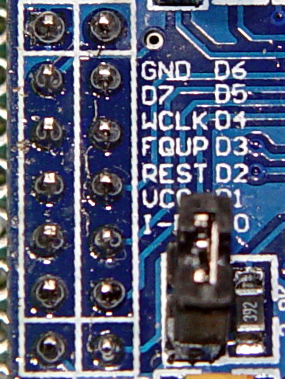
Yup, the D7 and GND pins are reversed.
Some careful probing showed the silkscreen is correct: the pins are, in fact, correctly labeled.
Should you be laying out a PCB in the expectation of using any DDS module from the lowest-price supplier, remember this high truth: Hell hath no fury like that of an unjustified assumption.
Fortunately, I’m hand-wiring the circuit and caught it prior to the smoke test.

Comments
5 responses to “Generic AD9850 DDS Modules: Beware Swapped D7 and GND Pins!”
I’m sure the good people of China gave you the correct schematic, it’s just that you’re not using the correct package for the J5 part – it’s the rare 1×7 pin header with swapped 6 and 7 pins :)
Well played, sir!
Wow – that’s a pretty nasty flaw. Was it an eBay purcbase direct from China?
Turns out I paid a bit more to get them direct from New York City, although there’s not a trace of doubt in my mind concerning their actual origin.
I now see a newer (?) layout with the parallel input pins lined up on one header and everything else on another, at a price 3 dB down from previous levels. It must be better!
[…] Yup, swapped VCC and GND pins. I should be used to that by now. […]