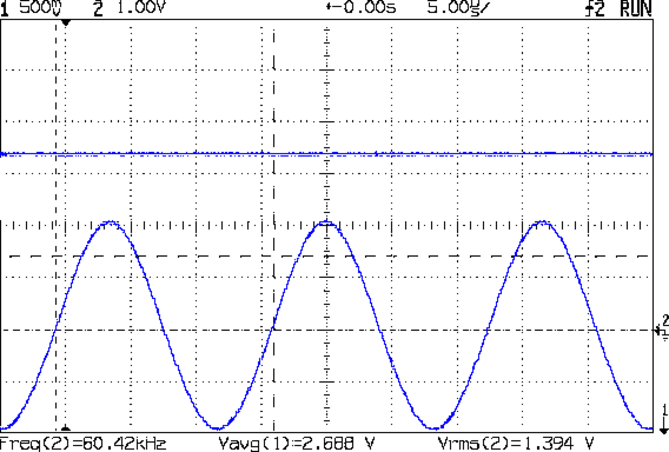
The part I didn’t understand turned out to be the bandwidth of the final output stage = “video bandwidth”, which defaults to 25 MHz. After fixing the input circuitry, a 25 MHz VBW let the output track a 60 kHz input signal just fine:

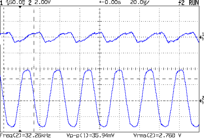
Adding a 56 nF cap across the C6 terminals (just above the AD8310) lowered the VBW to about 1 kHz:

Which flattened that sucker right out:
The ripple for an absurdly high amplitude 32 kHz signal amounts to 36 mV:
Firing the tracking generator into the input with a frequency sweep from 100 kHz to 250 MHz shows the low end looks much better:
There’s a slight droop across the sweep that might amount to 50 mV = 2 dB, which I’m inclined to not worry about in this context.
Applying the attenuators once again produces a scale factor of 23.5 mV/dB across 30 dB of RF, but this time the 60 kHz output makes sense, too.
Using the typical output curve from AN-691, that 2.0 V output corresponds to -13 dBm, which sounds about right for the tracking generator (which might really be -10 dBm).
I must calibrate the log amp output to find the actual intercept point (nominally -95 dBm, but could range from -86 to -102) at 60 kHz. The intercept is the extrapolated RF input producing 0 V out, which then acts as an offset for the voltage-to-dBm calculation; you start by finding the slope of the voltage vs. dBm line at some convenient power levels, then solve for dBm with V=0.
So a cheap AD8310 Log Amp module from eBay can work in the LF band, after you rearrange the input circuitry and tweak the chip’s filters. At least now I have a better understanding of what’s going on …

Comments
7 responses to “AD8310 Log Amp Module: Video Bandwidth Rolloff”
Nice looking results, Ed.
I found a possible clue to why the original input topology was used — there is a somewhat similar part from AD, the AD8313 demodulating log amp, that recommends putting the termination resistor across the device input pins. Quoting from the “Input Coupling” section of the datasheet (page 16), “It is preferable to place the termination resistor directly across the input pins, INHI to INLO, where it lowers the possible deleterious effects of dc offset voltages on the low end of the dynamic range. At low frequencies, this may not be quite as beneficial, since it requires larger coupling capacitors.”
So maybe the layout person picked up the wrong data sheet and that is where the mistake crept in. Who knows.
Makes sense to me. The coupling caps in the AD8313 datasheet look like a few mΩ at 100 MHz (the low end of its range), not the tens-to-hundreds of Ω for the ones on the AD8310 board (at the frequencies I need), so they fade away against the terminator.
I suppose I’m just using the AD8310 circuit outside its “design range”, although obviously you can’t figure the range from the sticker atop the can.
[…] Update – The rest of the story: Corrected Input Circuit and Video Bandwidth Rolloff. […]
[…] This little bracket attaches to a proto board holder, with holes for M3 inserts to mount the AD8310 log amp module: […]
[…] too large 10 µF caps in the signal path, particularly right before the log amp input, although the video bandwidth hack on the AD8310 module may contribute to the problem. In any event, I can see the log amp output […]
[…] even though the AD8310 log amp module should be able to handle such a tiny signal, the MAX4255 amp provides 40 dB of gain (OK, just 39.8 […]
[…] pull the resonant peak to 60.000 kHz. Unfortunately, the cheery 76 dB level is relative to the AD8310‘s nominal -108 dBV intercept at 4 μV: the log amp sees 25 mV after the MAX4255 op amp […]