QRPme Pocket Pal II: RF Waveforms and Meter Test

The QRPme Pocket Pal II produces RF test signals in the 20 meter and 40 meter bands, both square-ish waves derived from its 14.31818 MHz oscillator-in-a-can:

QRPme 20 meter - clip leads
QRPme 20 meter – clip leads

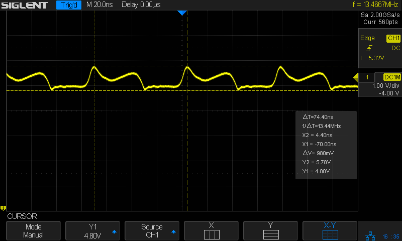
That’s the 20 meter signal, seen through the twisted pair test lead with alligator clips clamped on the scope probe, thusly:

QRPme Pocket Pal II - clip leads to probe tip
QRPme Pocket Pal II – clip leads to probe tip

When you’re working with RF signals, the “ground” part of the probe circuit matters:

QRPme 20 meter - probe tip gnd
QRPme 20 meter – probe tip gnd

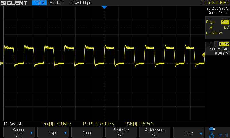
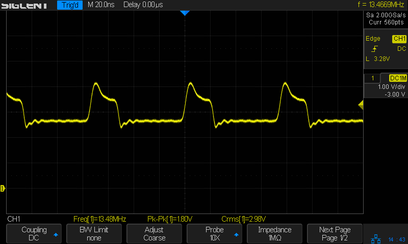
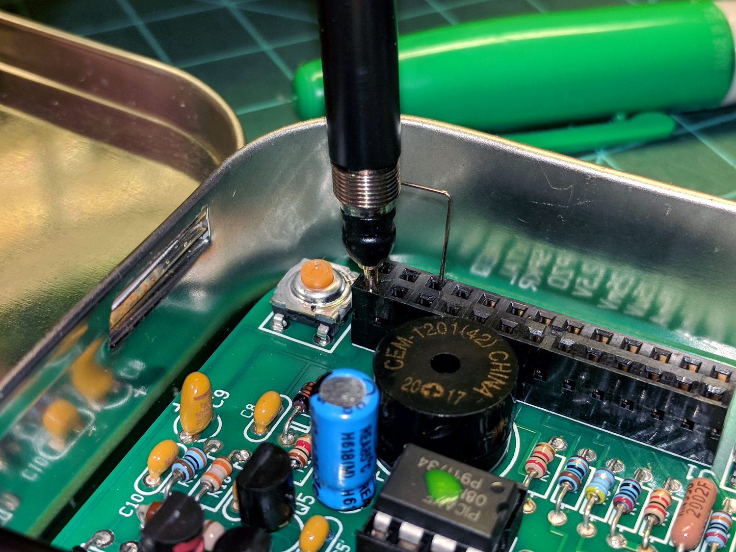
That’s with the probe and its short spring ground jammed directly into the header:

QRPme Pocket Pal II - probe tip gnd
QRPme Pocket Pal II – probe tip gnd

Well, in this case, signal quality doesn’t matter very much, as you’re using the Pocket Pal II at a hamfest (or your bench) to determine if an HF radio is completely dead.

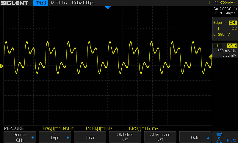
Here’s the 40 meter output, with the J3 jumper in place and the probe jammed into the header:

QRPme 40 meter - J3 on - probe tip gnd
QRPme 40 meter – J3 on – probe tip gnd

Pulling the J3 jumper off doubles the test signal amplitude:

QRPme 40 meter - J3 off - probe tip gnd
QRPme 40 meter – J3 off – probe tip gnd

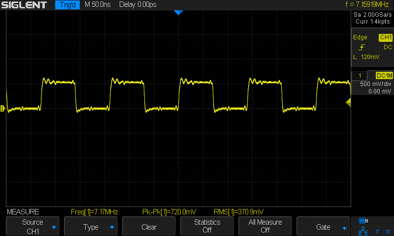
Nothing wrong with those signals! In a pinch, those edges probably produce harmonics up in the UHF bands.

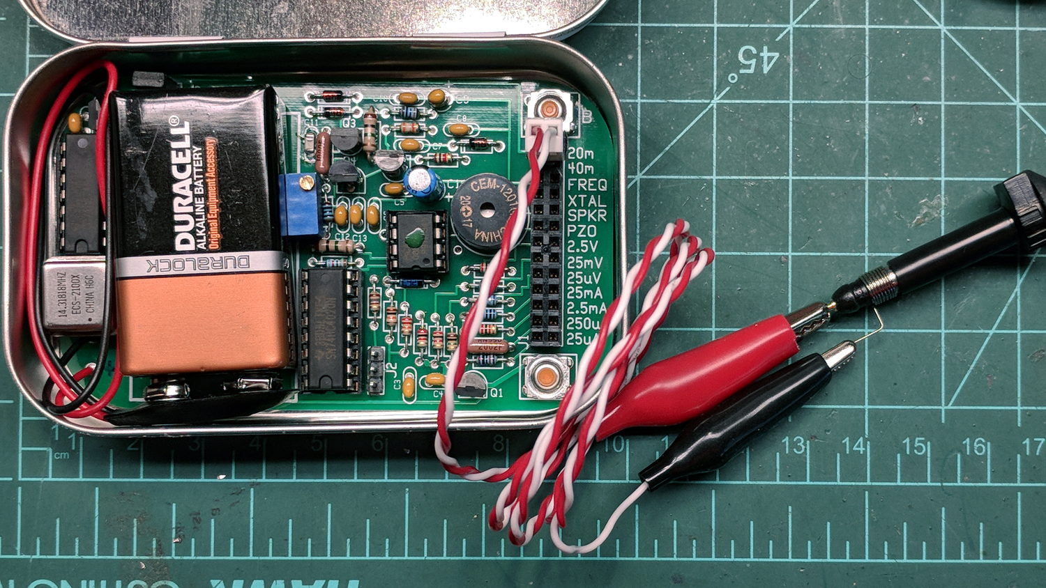
For completeness, here’s the 250 μA DC output driving a contestant chosen from the Box o’ Meters:

QRPme Pocket Pal II - 250 uA meter test
QRPme Pocket Pal II – 250 uA meter test

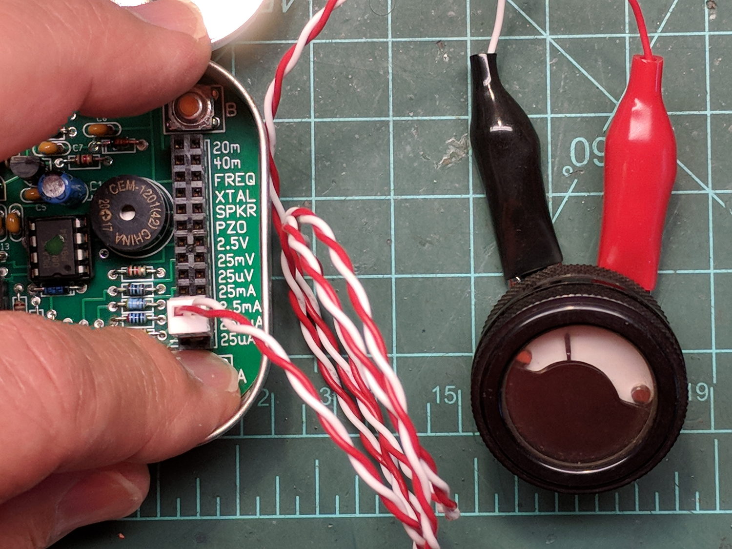
Eyeballometrically, the meter wants to see 1 mA for full-scale deflection, which is the whole point of the tester.

Recommended, with some early notes.

FM DDS: First Light Hardware

Some Barely Viable Prototype hardware for a frequency modulated DDS to replace Channel Elements requiring now-unobtainable crystals:

FM DDS - First Light layout
FM DDS – First Light layout

The heatsink (surely harvested from a PC, then salvaged from a box o’ goodies) runs about 25 °C above ambient while dropping a 12 V input to 5 V at 180 mA, so it’s good for maybe 2°C/W. It carries a KA278RA05C LDO regulator; you’d probably want something fancier in real life.

The AD9851 DDS requires a 5 V supply to run at 180 MHz from the 30 MHz oscillator on its PCB, with the side effect of putting its minimum Logic 1 Voltage threshold at 3.5 V. Because the Teensy 3.6 runs at 3.3 V from its own on-board linear regulator, the DIP 74AHCT125 level shifter between the two boosts the Teensy’s LVCMOS SPI signals to good old TTL.

The sticker on the CPU reminds me of the jumper cut between the USB +5 V line and the VIN pin, thus putting the Teensy on the better-regulated local supply for the benefit of its ADC reference:

Teensy 3.6 Back - VIN to VUSB jumper
Teensy 3.6 Back – VIN to VUSB jumper

The picture comes from PJRC’s exceedingly helpful Teensy 3.6 reference cards.

I ran header pins along both sides of the Teensy to simplify attaching scope probes and suchlike; the dangling gray wire brings the scope’s Arbitrary Function generator signal to the Teensy’s A9 input.

The FMDDS Mock 3 firmware lit right up, albeit with the faceplant of sending the SPI bytes in the wrong order and the wrong bit direction, which was easily fixed after a bit of puzzling:

FM DDS 10 MHz - SPI 16 MHz LSB
FM DDS 10 MHz – SPI 16 MHz LSB

Just a typo, could happen to anyone …

LXI-Tools for Siglent SDS2304X Oscilloscope and SDM3045X Multimeter

For whatever reason, my Siglent SDS2304X Oscilloscope and SDM3045X Multimeter partially implement their documented command sets through partial implementations of the VXI instrumentation driver network protocol. The Linux command-line side comes from lxi-tools, which one must fetch from its repository and compile from source(do liblxi first, then lxi-tools)  through the usual ./configure - make - sudo make install process, after tediously installing whatever dependencies might be revealed by incremental progress through the configuration(s) on your system(s).

The alternative, of course, is Labview on Windows.

The SDS2304X scope doesn’t respond to the LXI discover broadcast, so you must know and specify its IP address in the command. It’s easiest to configure the Siglent instruments at fixed IP addresses and be done with it:

lxi scpi -a 192.168.1.41 "*idn?"
Siglent Technologies,SDM3045X,SDM34whatever,5.01.01.03
lxi scpi -a 192.168.1.42 "*idn?"
*IDN SIGLENT,SDS2304X,SDS2Xwhatever,1.2.2.2 R10

Although the LXI tools also come in a Snap package, installing them that way prevents storing files outside the user’s home directory; having evolved a fairly extensive NFS filesystem, Snaps seem basically useless for my purposes. I don’t see much more security exposure from downloading and running a Snap than from downloading, compiling, and running the source code, but they obviously know what’s best for me.

QRPme Pocket Pal II

A QRPme Pocket Pal II could be a suitable project for a Squidwrench “advanced soldering” class:

QRPme Pocket Pal II - front
QRPme Pocket Pal II – front

Yes, it comes with a tin case:

QRPme Pocket Pal II - tin case
QRPme Pocket Pal II – tin case

You must fit your own insulating sheet under the PCB; polypropylene snipped from a retail package works fine.

It’s intended as a “mint tin sized tester for all kinds of hamfest goodies”, but it seems like a nice source of small currents, voltages, and signals suitable for stimulating all manner of circuitry one might encounter in later sessions of a beginning electronics class.

Before using it, of course, one must solder a handful of small through-hole parts into the PCB, a skill none of us were born with.

For completeness, the back side, hot from the soldering iron:

QRPme Pocket Pal II - rear
QRPme Pocket Pal II – rear

The kits (always buy two of anything like this) arrived minus a few parts, which I suspect was due to an avalanche of orders brought on by a favorable QST review. Fortunately, I (still) have a sufficient Heap o’ Parts to finish it off without resupply, although a hank of 9 V battery snaps will arrive in short order.

FM DDS: SPI Mock 3

Running some serial I/O in the background adds jitter to the timer interrupt pacing the ADC samples and as-yet-unwired DDS updates. For reference, an overview of the process showing the procession from the IRQ on the left to the SPI outputs near the middle and another IRQ on the far right:

DDS Mock - 0 VAC - SPI
DDS Mock – 0 VAC – SPI

Now, speed up the sweep and delay the trace by 25 μs to put the triggering pulse off-screen to the left and the second pulse at the center division:

ADC Sample IRQ jitter

The orange smear in the middle should be a tidy pulse, but it isn’t.

The  25 μs timer interrupt now has the highest priority on the front burner:

IntervalTimer AudioSampler;

... snippage ...

  AudioSampler.priority(0);
  if (!AudioSampler.begin(AudioSamplerIRQ, SamplePeriod)) {
    Serial.printf("Timer start failed\n");
    while (true) {
      FlipPin(BUILTIN_LED);
      delay(75);
    }
  }

Although nothing can interrupt it, other code / handlers may disable interrupts around their own critical sections and delay the tick. If the triggering tick (the off-screen one starting the trace) is delayed, then the on-screen pulse will appear “too soon”, to the left of center. If the triggering tick is on time, but the on-screen pulse is delayed, it’ll appear “too late” on the right.

The blur is (roughly) symmetric around the center graticule line, so the handwaving seems about right.

In round numbers, the jitter moves the interrupt ±325 ns on either side of its nominal position, with most of the pulses within ±100 ns. I doubt the jitter distribution is Gaussian, but vigorous handwaving says the RMS jitter might amount to 75 ns.

At the 4 kHz audio band limit, a 75 ns sampling error a phase error of 0.1°, so the maximum amplitude jitter would be sin(0.1°) = 0.002 = -55 dB, which might suffice for amateur-radio audio.

I think, anyhow.

FM DDS: Floating Point Timing

Inserting a few simple floating point operations between the SPI transfers provides a quick-n-dirty look at the timings:

Math timing - double ops
Math timing – double ops

The corresponding code runs in the ADC end-of-conversion handler:

void adc0_isr(void) {

  digitalWriteFast(ANALOG_PIN,HIGH);

  AnalogSample = adc->readSingle();                     // fetch just-finished sample

  SPI.beginTransaction(SPISettings(8000000, MSBFIRST, SPI_MODE0));
  digitalWriteFast(DDS_FQUD_PIN, LOW);

  SPI.transfer(DDSBuffer.Phase);                // interleave with FM calculations
  FlipPin(GLITCH_PIN);
  TestFreq += DDSStepFreq;
  FlipPin(GLITCH_PIN);
  SPI.transfer(DDSBuffer.Bits31_24);
  TestFreq -= DDSStepFreq;
  SPI.transfer(DDSBuffer.Bits23_16);
  TestFreq *= DDSStepFreq;
  SPI.transfer(DDSBuffer.Bits15_8);
  FlipPin(GLITCH_PIN);
  TestFreq /= DDSStepFreq;
  FlipPin(GLITCH_PIN);
  SPI.transfer(DDSBuffer.Bits7_0);
  SPI.endTransaction();                         // do not raise FQ_UD until next timer tick!

  digitalWriteFast(ANALOG_PIN,LOW);
}

The FlipPin() function twiddling the output bit takes a surprising amount of time, as shown by the first two gaps in the blocks of SPI clocks (D4). Some cursor fiddling on a zoomed scale says 300 ns = 50-ish cycles for each call. In round numbers, actual code doing useful work will take longer than that.

Double precision floating add / subtract / multiply seem to take about 600 ns. That’s entirely survivable if you don’t get carried away.

Double precision division, on the other paw, eats up 3 μs = 3000 ns, so it’s not something you want to casually plunk into an interrupt handler required to finish before the next audio sample arrives in 20 μs.

Overall, the CPU utilization seems way too high for comfort, mostly due to the SPI transfers, even without any computation. I must study the SPI-by-DMA examples to see if it’s a win.

Motorola K1003A Channel Element: Oscillation!

A handful of Motorola K1003A Receive Channel Elements arrived from eBay:

Motorola Channel Elements - overview
Motorola Channel Elements – overview

Having three 13466.666 kHz candidates, two with gold labels (2 ppm tempco) I disemboweled a silver-label (5 ppm) victim:

Motorola Channel Element - silver label
Motorola Channel Element – silver label

They’re well-studied, with readily available schematics:

k1003-schematic
k1003-schematic

For lack of anything smarter, I put a 1 kΩ resistor from RF Out to Ground to get some DC current going, then used a 470 nF cap and 47 Ω resistor as an AC load:

K1003 Channel Element - bias lashup
K1003 Channel Element – bias lashup

Which oscillated around a mid-scale DC bias, but looked ugly:

K1003 Channel Element - 13.4 MHz output - 1k bias
K1003 Channel Element – 13.4 MHz output – 1k bias

Perusing some receiver schematics suggested a heavier DC load, so I swapped in a 470 Ω resistor:

K1003 Channel Element - 470 ohm bias - 13.4 MHz output
K1003 Channel Element – 470 ohm bias – 13.4 MHz output

It’s now running around 3 V bias with fewer harmonics; the scope’s frequency display in the upper right corner seems happier, too.

The receiver will run that through a filter to wipe off the harmonics, then multiply the frequency by three to get the mixer LO.

There are many, many different Channel Elements out there, in receive and transmit flavors, but at least I have some idea what’s going on inside.