Some Barely Viable Prototype hardware for a frequency modulated DDS to replace Channel Elements requiring now-unobtainable crystals:

The heatsink (surely harvested from a PC, then salvaged from a box o’ goodies) runs about 25 °C above ambient while dropping a 12 V input to 5 V at 180 mA, so it’s good for maybe 2°C/W. It carries a KA278RA05C LDO regulator; you’d probably want something fancier in real life.
The AD9851 DDS requires a 5 V supply to run at 180 MHz from the 30 MHz oscillator on its PCB, with the side effect of putting its minimum Logic 1 Voltage threshold at 3.5 V. Because the Teensy 3.6 runs at 3.3 V from its own on-board linear regulator, the DIP 74AHCT125 level shifter between the two boosts the Teensy’s LVCMOS SPI signals to good old TTL.
The sticker on the CPU reminds me of the jumper cut between the USB +5 V line and the VIN pin, thus putting the Teensy on the better-regulated local supply for the benefit of its ADC reference:
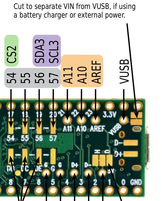
The picture comes from PJRC’s exceedingly helpful Teensy 3.6 reference cards.
I ran header pins along both sides of the Teensy to simplify attaching scope probes and suchlike; the dangling gray wire brings the scope’s Arbitrary Function generator signal to the Teensy’s A9 input.
The FMDDS Mock 3 firmware lit right up, albeit with the faceplant of sending the SPI bytes in the wrong order and the wrong bit direction, which was easily fixed after a bit of puzzling:
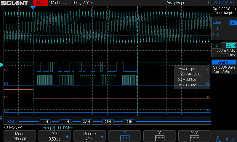
Just a typo, could happen to anyone …
