Ed Nisley's Blog: Shop notes, electronics, firmware, machinery, 3D printing, laser cuttery, and curiosities. Contents: 100% human thinking, 0% AI slop.
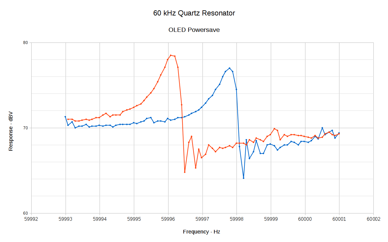
Disabling the display by activating its powersave option reveals 60 Hz pulses from the USB port on the Arduino Nano:
OLED Powersave – 60 Hz USB Ground Loop
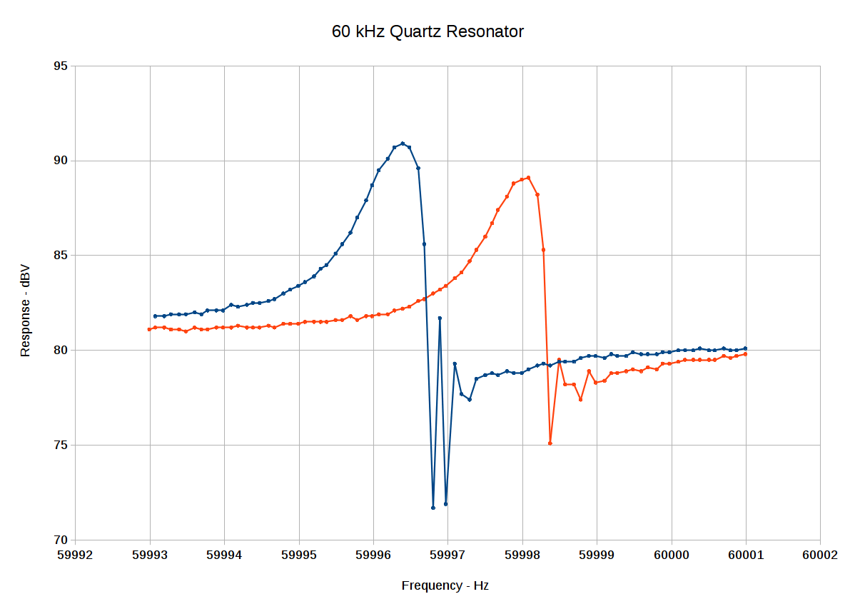
Unplugging the USB cable, leaving just the +5 VDC power supply and coax cable to the oscilloscope, solves most of the problem:
OLED Powersave – USB unplugged
A closer look shows some (relatively) low frequency noise remains in full effect:
OLED Powersave – USB unplugged – detail
Disabling the display while measuring the crystal seems sensible, although, to avoid surprises, a pushbutton should start the process. Unplugging the USB port puts a real crimp in the data collection, although that’s probably survivable with a USB isolator, one of which is on the way around the planet.
The remaining low-level chop requires more thought. Somewhat to my surprise, holding the Arduino Reset button down doesn’t change much of anything, so it’s not a firmware thing.
Those 10 µF coupling caps gotta go.
With the OLED dark and the USB carrying data:
Spectrum – OLED Powersave – USB in
Compare that to the first pass:
Spectrum-60
Tamping down the noise seems to reduce the overall amplitude variation, but it also makes the capacitor-in and capacitor-out curves more consistent. There may be other things going on that I haven’t accounted for.
The peak frequencies differ by 0.2 Hz, which is probably due to a few degrees of temperature difference. Obviously, it’s badly in need of a temperature calibration & correction.
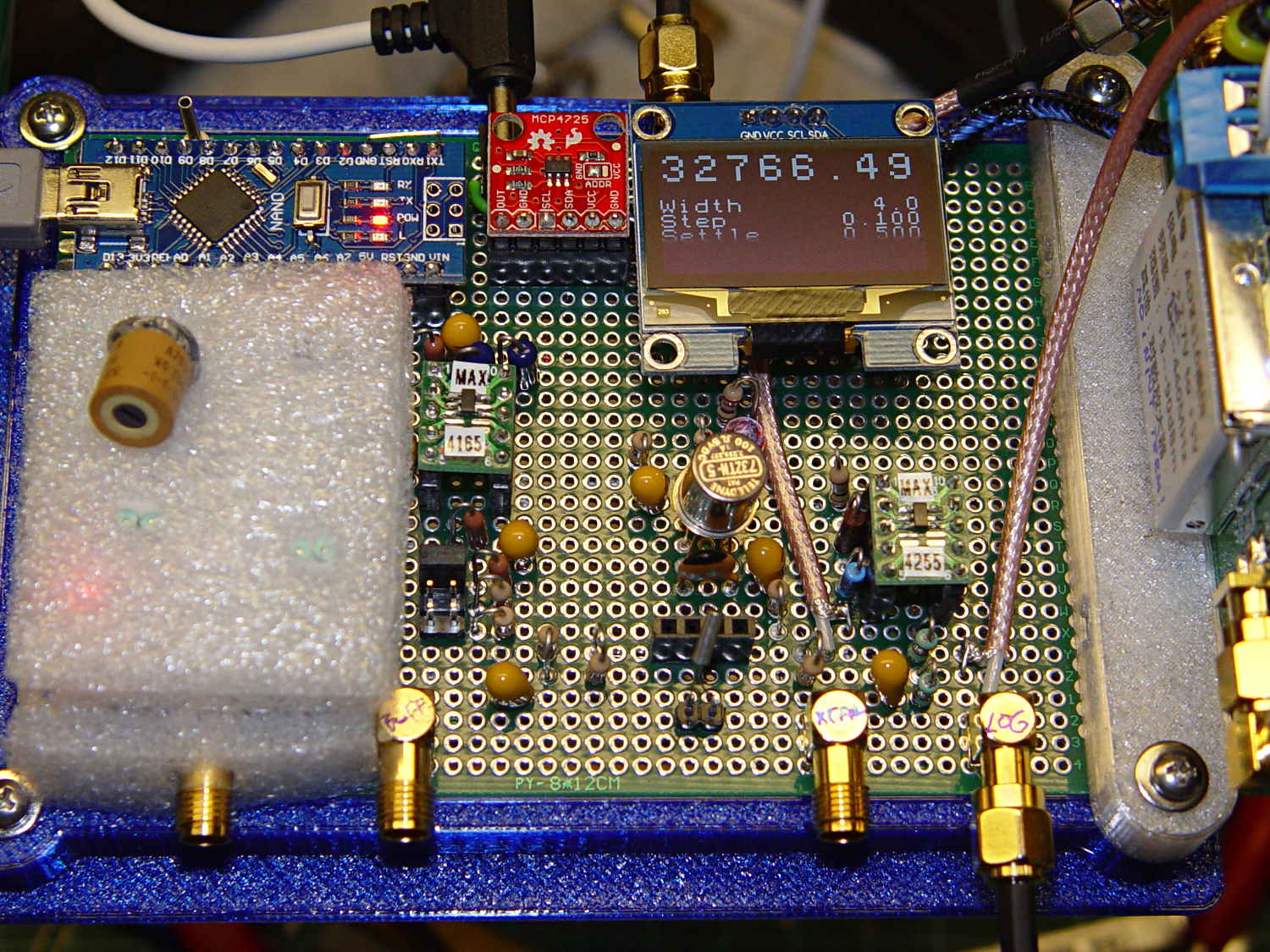
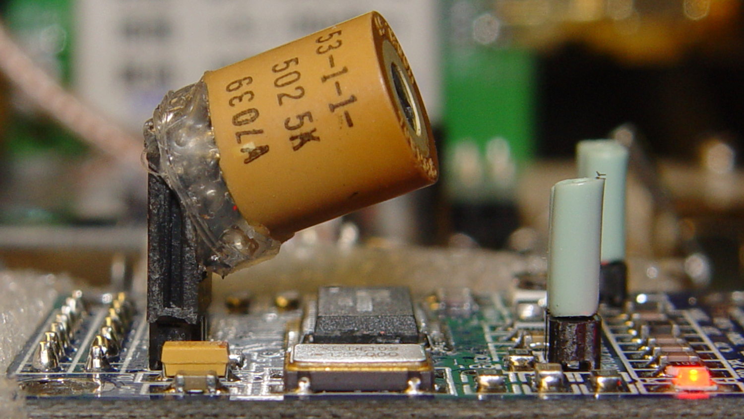
A strip of NXP (née Philips plus Freescale, including the part of Motorola that didn’t become ON) LM75A I²C temperature sensors arrived from beyond the horizon. To see if they worked, I soldered thin wires directly to the SO-8 pins, entombed it in Kapton tape to prevent spitzensparken, and jammed it under the foam insulation atop the AD9850 DDS module:
AD9850 DDS module with LM75A Temperature Sensor
This turns out to be easier than screwing around with thermistors, because the chip reports the temperature directly in Celcius with ⅛ °C resolution. Classic LM75 chips from National (now absorbed by TI) had ½ °C resolution, but the datasheet shows the bits have an easily extensible format:
LM75A Temperature Data Format
Huh. Fixed-point data, split neatly on a byte boundary. Who’d’a thunk it?
There’s a standard Arduino library using, naturally enough, floating point numbers, but I already have big fixed point numbers lying around and, with the I²C hardware up & running from the X axis DAC and OLED display, this was straightforward:
The next-to-last line squirts the temperature through the serial port to make those nice plots.
Casually ignoring all I²C bus error conditions will eventually lead to heartache and confusion. In particular, the Basement Laboratory temperature must never fall below 0 °C, because I just plunk the two’s-complement temperature data into an unsigned fixed point number.
Which produces the next-to-bottom line:
DDS OLED with LM75 temperature
Alas, the u8x8 font doesn’t include a degree symbol.
Given sufficient motivation, I can now calibrate the DDS output against the GPS-locked 10 MHz standard to get a (most likely) linear equation for the oscillator frequency offset as a function of temperature. The DDS module includes a comparator to square up its sine wave, so an XOR phase detector or something based on filtering the output of an analog switch might be feasible.
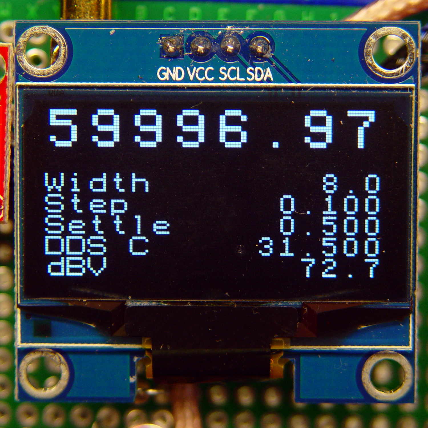
The crystal test fixture and amp huddle in front of the OLED display:
Crystal Tester – First Light
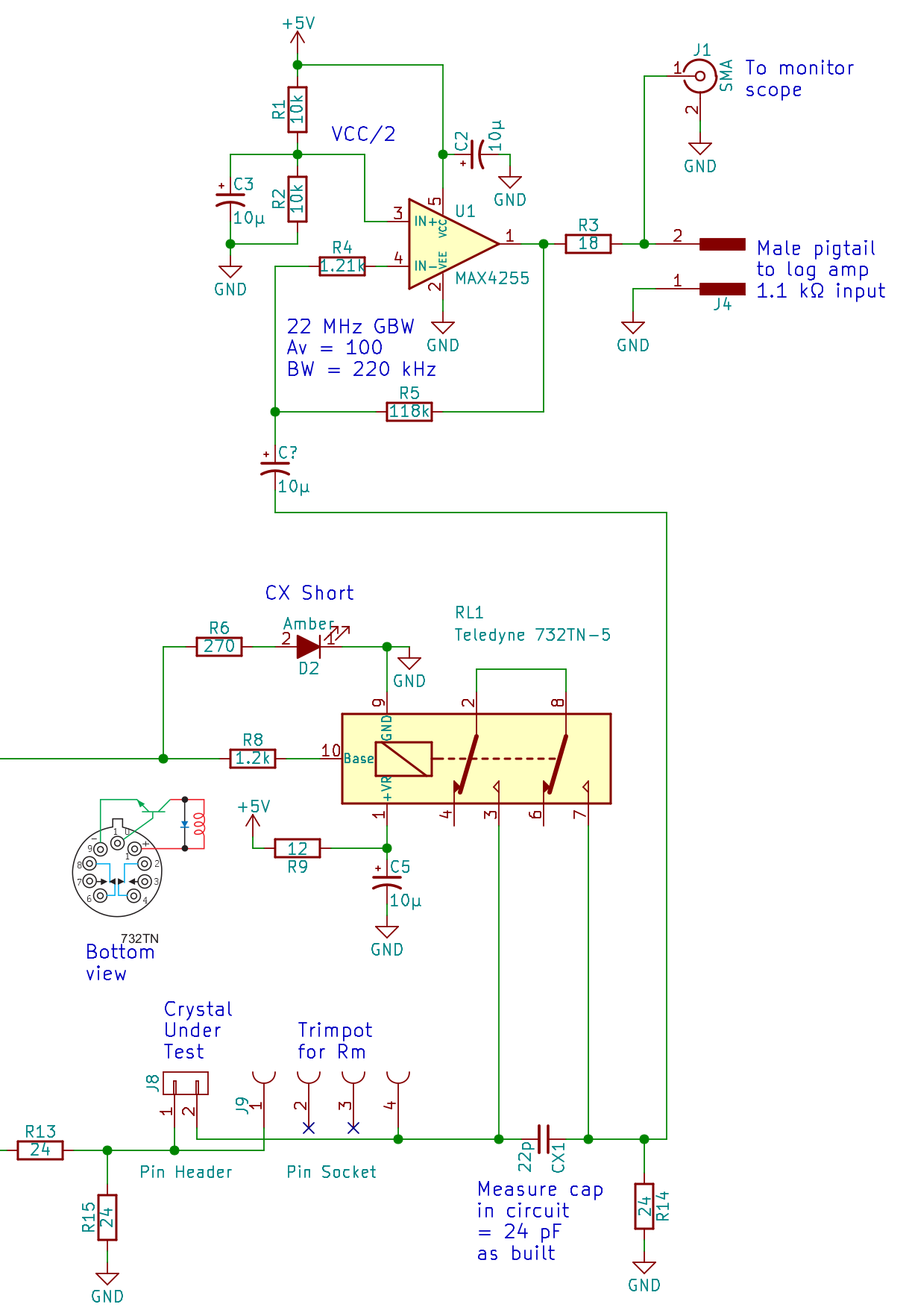
The schematic:
Test fixture – Relay – MAX4255 amp – schematic
The 22 pF cap now sits across the relay’s NO contacts, so as to simplify measuring the total in-circuit capacitance. The LED turns on when the relay shorts out the capacitor, which has a 50% probability of making more sense.
The quartz tuning fork resonators have an ESR around 20 or 30 kΩ, so the off-resonance output should be down something like -60 dB = 20 log (24 / 24×10³) from the 150 mV input: 200 µV (-ish). It’s actually around 1 mV, suggesting plenty of blowby through the baling-wire connections hidden under that neat top surface. I think that’s why the whole setup shows only about 8 dB of dynamic range; more attention to detail may be in order, although the peaks probably won’t move all that much.
Anyhow, even though the AD8310 log amp module should be able to handle such a tiny signal, the MAX4255 amp provides 40 dB of gain (OK, just 39.8 dB) and rolls off the high end at 220 kHz as a side benefit of its 22 MHz GBW.
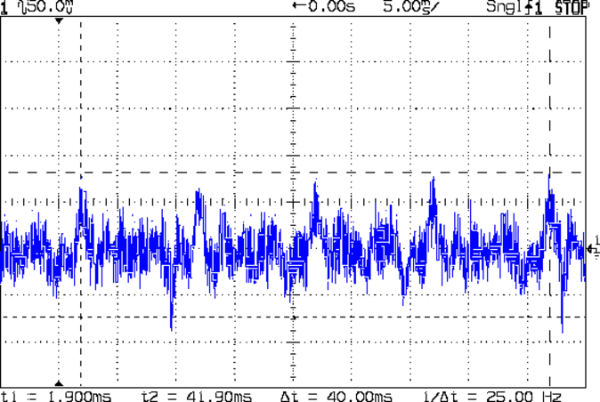
There’s way too much low frequency rumble at the amp output:
100 Hz noise at MA4255 output
What look like grass is actually the 60 kHz resonator output: those big lumps & bumps are noise from this-and-that. The repetitive peaks and dents exactly 10 ms apart (the cursors span four of ’em) felt a lot like OLED refresh cycles and, indeed, went away when I yanked the display out. Pulling the USB connection eliminates another tremendous heap o’ noise, so there’s likely a ground loop (-ish) thing going on, too. This may call for a USB optical isolator, its commercial equivalent, or more eBay offerings. Getting rid of that junk may improve the dynamic range enough to keep me from doing anything drastic.
The AD8310 log amp input now has decent coupling caps, so it’s not seeing the VCC/2 bias, and I removed that kludged-in 50 Ω terminating resistor to present its full 1.1 kΩ input resistance to the op amp.
The Big Ideas: the DDS output, being more-or-less constant, needs a variable-gain amp to set the crystal drive level. The amp also fixes the impedance mismatch between the DDS output and the crystal, which may not be much of a problem for the (very) high ESR quartz tuning fork resonators in play.
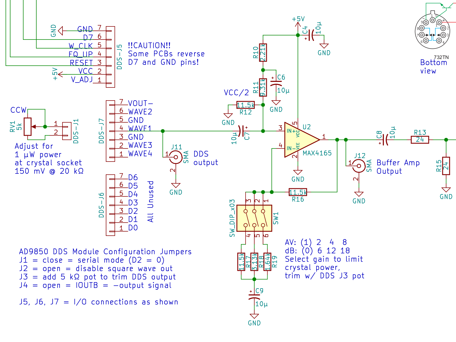
The AD9850 DDS output feeds a 70 MHz (-ish) elliptical reconstruction filter chopping off image frequencies descending from the 125 MHz sampling clock, with a 100 Ω (-ish) output impedance that’s just about purely resistive at 60 kHz. An on-board 3.9 kΩ resistor (labeled with 392 on their schematic) sets the full-scale output current to 10 mA for a peak voltage of 1 V. The module uses only the + output of the differential pair, which means the sine wave runs from 0 V to 1 V: 1 Vpp = 500 mVpeak = 353 mVrms (ignoring the 500 mV offset).
Pin header J3 normally sports a jumper to connect the 3.9 kΩ RSET resistor, but you can insert an external resistor to increase the resistance and decrease the output current:
IOUT = 32 × 1.248 V / RSET
A little hot-melt glue action produced a suitable lashup from a 5 kΩ trimpot:
AD9850 DDS Module – 5 k external RSET trimpot
The pillars of green wire insulation forestall screwdriver shorts to the bare pin headers, although that’s less of risk with the upper insulating foam sheet in place:
Crystal Tester – First Light
A 5 kΩ trimpot can vary the output voltage downward by a factor of 2 = -6 dB, more or less.
All the quartz tuning fork resonator specs I’ve found, none of which may apply to the units on hand, seem to require no more than 1 µW drive. Given a resonator’s equivalent series resistance of around 20 kΩ (for real!), the drive voltage will be 150 mV (-ish):
1 µW = V² / 20 kΩ, so V = sqrt(20×10³) = 141 mV
The nominal version of the crystal tester had a 50 Ω input impedance, so I picked a MAX4165 op amp with mojo sufficient for anything over 25 Ω; in retrospect, a lighter load than 48 Ω would be fine.
In any event, the amp looks like this:
MAX4165 Buffer Amp
What looks like a DIP switch is really the 3×2 jumper header just to the right of the foam insulation, in front of the SOT23 space transformer PCB carrying the MAX4165. No jumper = 0 dB gain, then 6 dB steps upward from there. The -6 dB trimpot range gives more-or-less continuous output tweakage across 24 dB, -6 dB to +18 dB, which is certainly excessive. The 24 Ω terminating resistors provide 6 dB loss into the crystal, so the effective range is -12 to +12 dB, with 0 dB = 350 mVrms and -6 dB = 150 mVrms (-ish) at the crystal.
It’s a non-inverting amplifier, which (also in retrospect) probably isn’t a win:
Yet Another Bypass Cap on the cold end of the gain-setting resistors
Overly elaborate VCC/2 biasing to maintain sufficiently high input impedance
I’m reasonably sure all those big caps contribute to some low-level motorboating, but haven’t tracked it down.
A slight modification spits out the (actual) frequency and dBV response (without subtracting the 108 dB intercept to avoid negative numbers for now) to the serial port in CSV format, wherein a quick copypasta into a LibreOffice Calc spreadsheet produces this:
Spectrum-32
Changing the center frequency and swapping in a 60 kHz resonator:
Spectrum-60
Much prettier than the raw scope shot with the same data, there can be no denyin’:
Log V vs F – 32766 4 Hz – CX overlay
I think the wobbulations around the parallel resonant dip come from the excessively hugely too large 10 µF caps in the signal path, particularly right before the log amp input, although the video bandwidth hack on the AD8310 module may contribute to the problem. In any event, I can see the log amp output wobbling for about a second, which is way too long.
Anyhow, the series-resonant peaks look about 1 Hz wide at the -3 dBV points, more or less agreeing with what I found with the HP 8591 spectrum analyzer. The series cap is a bit smaller, producing a slightly larger frequency change in the series resonant frequency: a bit under 2 Hz, rather than the 1 Hz estimated with the function generator and spectrum analyzer.
I still don’t understand why the parallel resonant dip changes, although I haven’t actually done the pencil pushing required for true understanding.
The ample padding around this bag of fragile pecans leaves nothing to be desired:
Amazon – well-packed pecans
They’re firmly held in place on all sides, well protected from injury, and survived their shipping ordeal unscathed: not a bruise or break to be found. Well done!
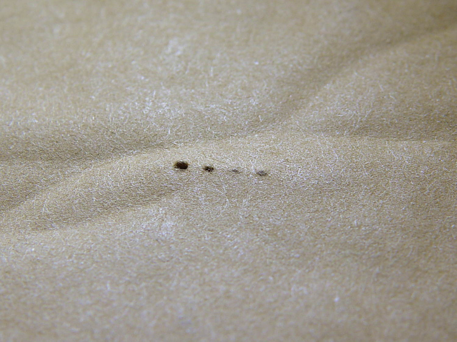
That’s not always the case. A padded envelope recently arrived with an obvious wound:
Amazon – envelope perforations
Which came from its completely unprotected contents:
Amazon – unprotected PCB pins
Fortunately, the fragile glass front plate of that OLED managed to put itself flat against a small box inside the otherwise empty bag. it wasn’t broken, but due only to good fortune.
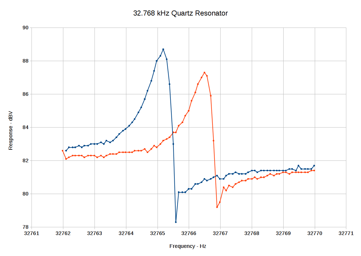
After adding a MAX4165 buffer amp to drive the crystal test fixture at 1 µW and a MAX4255 to amplify the 1 mV crystal output by 40 dB, then removing the AD8310 log amp module’s 50 Ω terminator to better match the MAX4255’s output drive ability, this happened:
Log V vs F – 32766 4 Hz – CX overlay
That’s:
A 32.768 kHz quartz resonator
A ±2 Hz span centered on 32.766 kHz
0.10 Hz frequency steps
The 22 pF cap out / in circuit (left & right peaks, respectively)
Log amp output at 24 mV/dBV, with a nominal -108 dBV intercept at 0 V
With a 4 Hz span and 0.1 Hz steps, you get only 41 samples along the X axis: it’s supposed to look spotty.
The 2.2 V response at the top of the left peak corresponds to 2.2 / 24 mV/dBV = 91.7 dBV, then you knock off the -108 dBV intercept to get -16.3 dBV. The valley at 1.88 V is 78.3 – 108 = -29.7 dBV, down about 13 dBV from the corresponding peak. The peak-to-baseline over on the right looks like 200 mV = 8 dBV.
The AD8310 datasheet uses “intercept” in a manner I had not previously encountered. They plot the AD8310 output in volts against the input signal level in dBV, with the “intercept” marking the extrapolated point where the straight line with slope 24 mV/dBV crosses the X axis: the equation is volts = slope*(input dBV – intercept dBV). Back in the day, I learned the intercept was where the line crossed the Y axis at X=0, so the straight-line equation was simply y = slope*x + intercept. Took me a while to figure that out.
Then subtract the 40 dB gain from the crystal output to the log amp to get -56 dbV = 1.6 mV. That’s close enough to the 1 mV before adding the MAX4255. All those numbers seem slightly squishy, but they’re close enough.
The peaks are 13-ish spots apart, which corresponds to 1.3 Hz, which is roughly the 1 Hz I measured with the HP8591 spectrum analyzer. The baseline is down 8 dBV, not quite as much as the analyzer’s 13 dB at 1 Hz offset from the peaks.
What’s not right: the parallel-resonant dip to the right of each peak should be at the same frequency for both traces, because it doesn’t vary with added series capacitance, but it’s pretty much tracking the series-resonant peak frequency.
The amount of noise on the log amp output looks like 50 mV = 2 dBV. That’s a lot, compared to the 13 dBV response, but some judicious averaging may save the day.
The 22 MHz GBW of the MAX4255 rolls off the high end at 220 kHz. I AC coupled the signal chain with 10 µF dipped tantalum caps from my lifetime supply, which may pass entirely too much of the low end; the settling time is way too long. This probably requires smaller caps and maybe an actual bandpass filter.
The 50 mV-ish noise on the DAC output driving the X axis suggests my proto board layout isn’t up to the demands of this circuit: there shouldn’t be any noise in that direction.
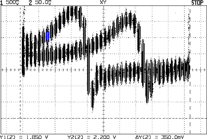
Some poking around suggests the OLED display is way noisier than you’d (well, I’d) expect. The faded-out lower section in the picture below suggests it’s refreshing one line = 128 pixels at a time. More study is indicated.
But, if you squint hard enough, this lashup produces numbers in the right ballpark. Given that it’s a collection of cheap-as-dirt eBay modules flying in formation, that’s nothing to sniff at:
Crystal Tester – First Light
Those “gold tone” SMA connectors really make it look like serious RF hardware, don’t they? [grin]
The round twiddlepot floating on the white pillow trims the DDS output voltage by a factor of two = 6 dB. Combined with the 0-6-12-18 dB gain steps provided by the header in front of the MAX4165 (to the right of the pillow), you can set the drive voltage so the crystal gets (roughly) its rated 1 µW maximum drive power.