The Big Ideas: the DDS output, being more-or-less constant, needs a variable-gain amp to set the crystal drive level. The amp also fixes the impedance mismatch between the DDS output and the crystal, which may not be much of a problem for the (very) high ESR quartz tuning fork resonators in play.
The AD9850 DDS output feeds a 70 MHz (-ish) elliptical reconstruction filter chopping off image frequencies descending from the 125 MHz sampling clock, with a 100 Ω (-ish) output impedance that’s just about purely resistive at 60 kHz. An on-board 3.9 kΩ resistor (labeled with 392 on their schematic) sets the full-scale output current to 10 mA for a peak voltage of 1 V. The module uses only the + output of the differential pair, which means the sine wave runs from 0 V to 1 V: 1 Vpp = 500 mVpeak = 353 mVrms (ignoring the 500 mV offset).
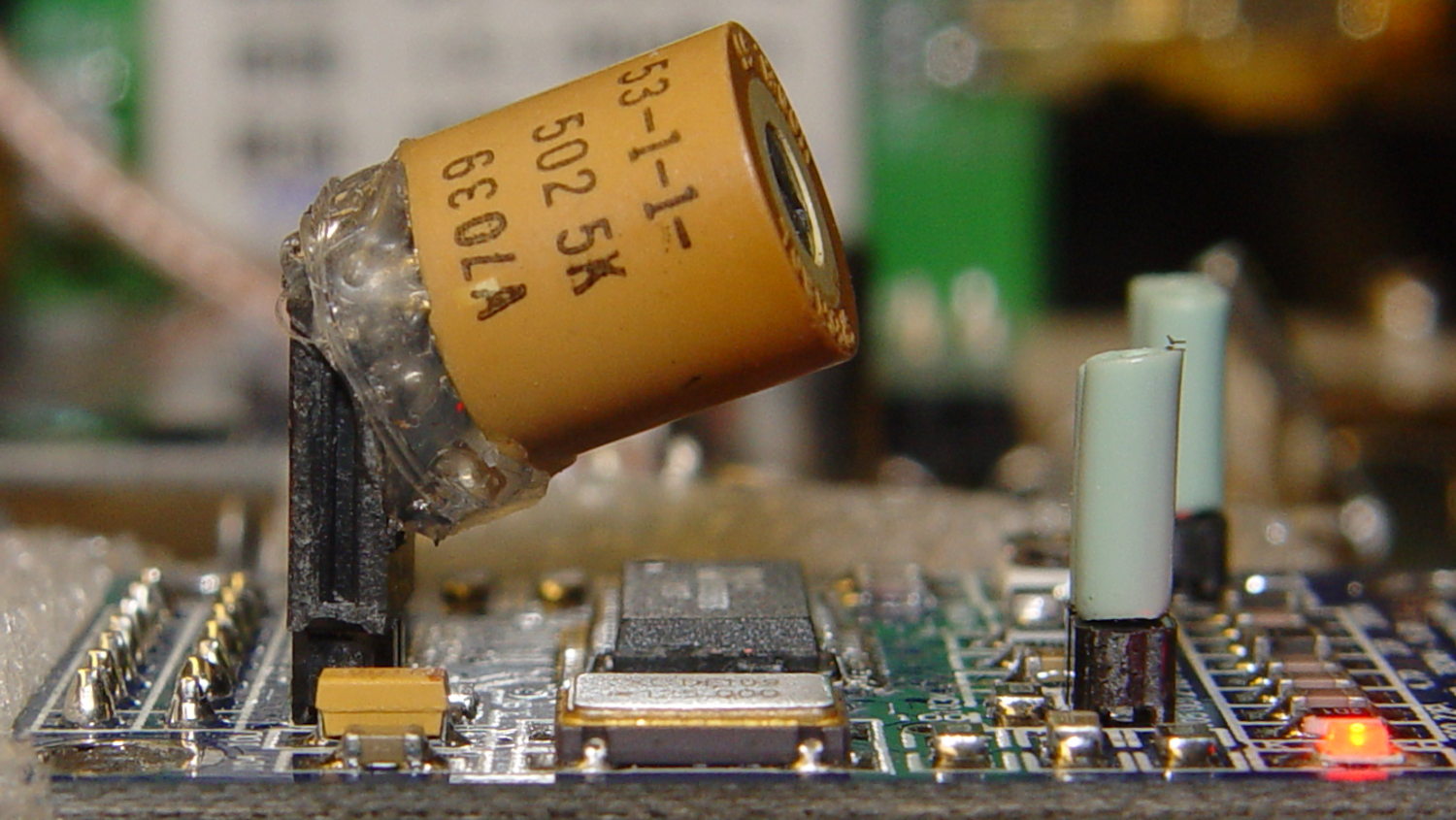
Pin header J3 normally sports a jumper to connect the 3.9 kΩ RSET resistor, but you can insert an external resistor to increase the resistance and decrease the output current:
IOUT = 32 × 1.248 V / RSET
A little hot-melt glue action produced a suitable lashup from a 5 kΩ trimpot:
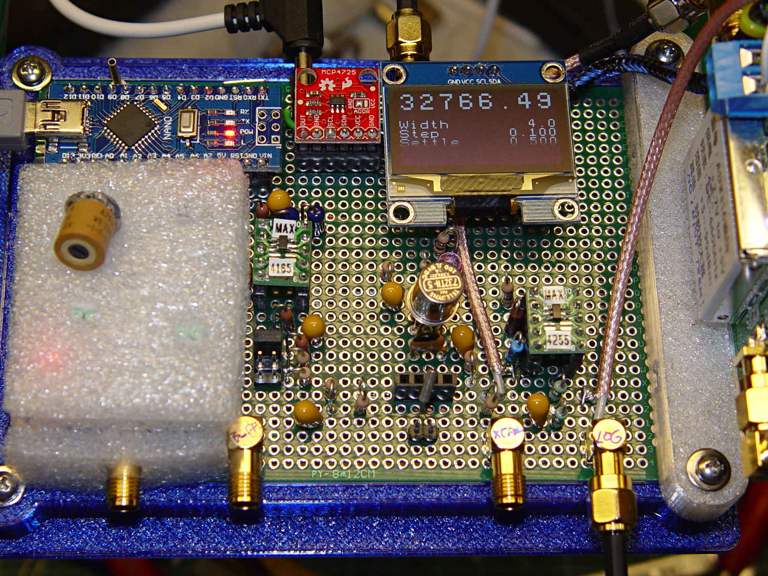
The pillars of green wire insulation forestall screwdriver shorts to the bare pin headers, although that’s less of risk with the upper insulating foam sheet in place:
A 5 kΩ trimpot can vary the output voltage downward by a factor of 2 = -6 dB, more or less.
All the quartz tuning fork resonator specs I’ve found, none of which may apply to the units on hand, seem to require no more than 1 µW drive. Given a resonator’s equivalent series resistance of around 20 kΩ (for real!), the drive voltage will be 150 mV (-ish):
1 µW = V² / 20 kΩ, so V = sqrt(20×10³) = 141 mV
The nominal version of the crystal tester had a 50 Ω input impedance, so I picked a MAX4165 op amp with mojo sufficient for anything over 25 Ω; in retrospect, a lighter load than 48 Ω would be fine.
In any event, the amp looks like this:
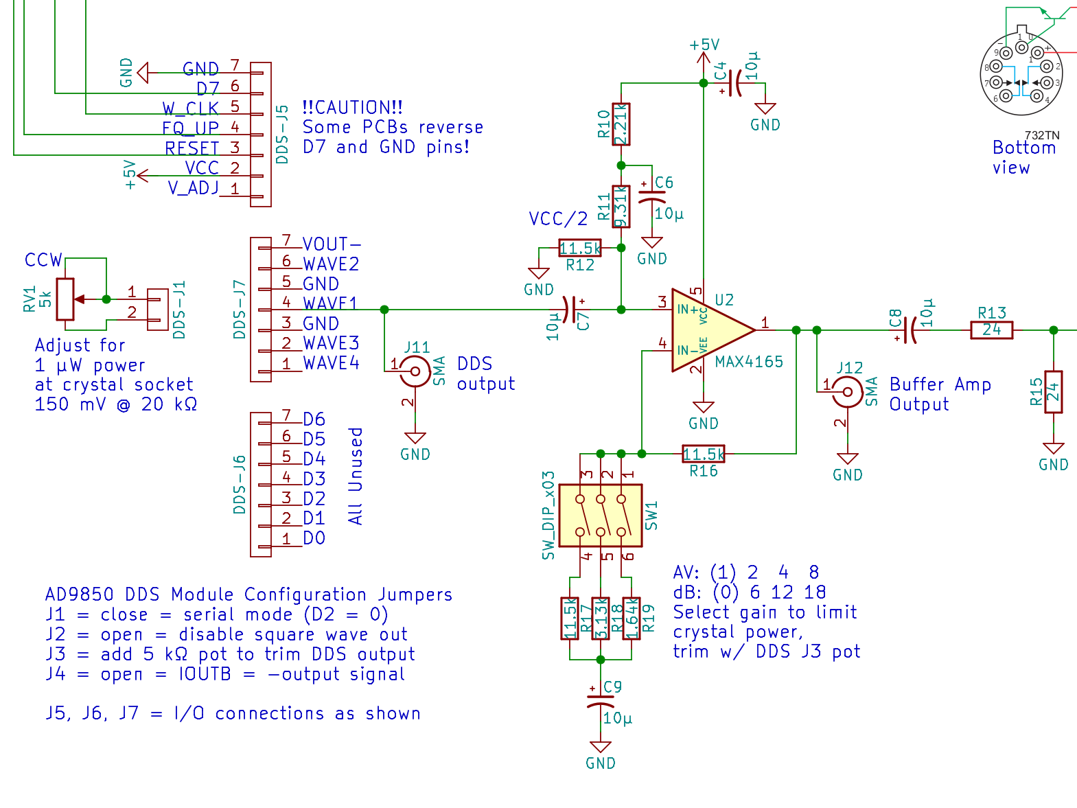
What looks like a DIP switch is really the 3×2 jumper header just to the right of the foam insulation, in front of the SOT23 space transformer PCB carrying the MAX4165. No jumper = 0 dB gain, then 6 dB steps upward from there. The -6 dB trimpot range gives more-or-less continuous output tweakage across 24 dB, -6 dB to +18 dB, which is certainly excessive. The 24 Ω terminating resistors provide 6 dB loss into the crystal, so the effective range is -12 to +12 dB, with 0 dB = 350 mVrms and -6 dB = 150 mVrms (-ish) at the crystal.
It’s a non-inverting amplifier, which (also in retrospect) probably isn’t a win:
- Yet Another Bypass Cap on the cold end of the gain-setting resistors
- Overly elaborate VCC/2 biasing to maintain sufficiently high input impedance
I’m reasonably sure all those big caps contribute to some low-level motorboating, but haven’t tracked it down.

Comments
3 responses to “LF Crystal Tester: DDS Buffer Amp”
[…] is the GPS-locked 10 MHz reference, the lower trace is the AD9850 DDS output (not through the MAX4165 buffer amp, because bandwidth). If the frequencies aren’t identical, the DDS trace will crawl left or […]
[…] no amplitude adjustment, other than the DDS current-control twiddlepot and the buffer amp’s gain-setting jumpers, but I (think I can) gimmick up an adequate […]
[…] alligator clips come from the LF Crystal Tester‘s buffer amp, with the Arduino Nano loaded with sine generator firmware. A 100 nF cap blocks […]