The Smell of Molten Projects in the Morning

Ed Nisley's Blog: Shop notes, electronics, firmware, machinery, 3D printing, laser cuttery, and curiosities. Contents: 100% human thinking, 0% AI slop.

Tag: Arduino

All things Arduino

  • LF Crystal Tester: Pretty Plots

    A slight modification spits out the (actual) frequency and dBV response (without subtracting the 108 dB intercept to avoid negative numbers for now) to the serial port in CSV format, wherein a quick copypasta into a LibreOffice Calc spreadsheet produces this:

    Spectrum-32
    Spectrum-32

    Changing the center frequency and swapping in a 60 kHz resonator:

    Spectrum-60
    Spectrum-60

    Much prettier than the raw scope shot with the same data, there can be no denyin’:

    Log V vs F - 32766 4 Hz - CX overlay
    Log V vs F – 32766 4 Hz – CX overlay

    I think the wobbulations around the parallel resonant dip come from the excessively hugely too large 10 µF caps in the signal path, particularly right before the log amp input, although the video bandwidth hack on the AD8310 module may contribute to the problem. In any event, I can see the log amp output wobbling for about a second, which is way too long.

    Anyhow, the series-resonant peaks look about 1 Hz wide at the -3 dBV points, more or less agreeing with what I found with the HP 8591 spectrum analyzer. The series cap is a bit smaller, producing a slightly larger frequency change in the series resonant frequency: a bit under 2 Hz, rather than the 1 Hz estimated with the function generator and spectrum analyzer.

    I still don’t understand why the parallel resonant dip changes, although I haven’t actually done the pencil pushing required for true understanding.

    Ain’t they lovely, though?

  • LF Crystal Tester: First Light!

    After adding a MAX4165 buffer amp to drive the crystal test fixture at 1 µW and a MAX4255 to amplify the 1 mV crystal output by 40 dB, then removing the AD8310 log amp module’s 50 Ω terminator to better match the MAX4255’s output drive ability, this happened:

    Log V vs F - 32766 4 Hz - CX overlay
    Log V vs F – 32766 4 Hz – CX overlay

    That’s:

    • A 32.768 kHz quartz resonator
    • A ±2 Hz span centered on 32.766 kHz
    • 0.10 Hz frequency steps
    • The 22 pF cap out / in circuit (left & right peaks, respectively)
    • Log amp output at 24 mV/dBV, with a nominal -108 dBV intercept at 0 V

    With a 4 Hz span and 0.1 Hz steps, you get only 41 samples along the X axis: it’s supposed to look spotty.

    The 2.2 V response at the top of the left peak corresponds to 2.2 / 24 mV/dBV = 91.7 dBV, then you knock off the -108 dBV intercept to get -16.3 dBV. The valley at 1.88 V is 78.3 – 108 = -29.7 dBV, down about 13 dBV from the corresponding peak. The peak-to-baseline over on the right looks like 200 mV = 8 dBV.

    The AD8310 datasheet uses “intercept” in a manner I had not previously encountered. They plot the AD8310 output in volts against the input signal level in dBV, with the “intercept” marking the extrapolated point where the straight line with slope 24 mV/dBV crosses the X axis: the equation is volts = slope*(input dBV – intercept dBV). Back in the day, I learned the intercept was where the line crossed the Y axis at X=0, so the straight-line equation was simply y = slope*x + intercept. Took me a while to figure that out.

    Then subtract the 40 dB gain from the crystal output to the log amp to get -56 dbV = 1.6 mV. That’s close enough to the 1 mV before adding the MAX4255. All those numbers seem slightly squishy, but they’re close enough.

    The peaks are 13-ish spots apart, which corresponds to 1.3 Hz, which is roughly the 1 Hz I measured with the HP8591 spectrum analyzer. The baseline is down 8 dBV, not quite as much as the analyzer’s 13 dB at 1 Hz offset from the peaks.

    What’s not right: the parallel-resonant dip to the right of each peak should be at the same frequency for both traces, because it doesn’t vary with added series capacitance, but it’s pretty much tracking the series-resonant peak frequency.

    The amount of noise on the log amp output looks like 50 mV = 2 dBV. That’s a lot, compared to the 13 dBV response, but some judicious averaging may save the day.

    The 22 MHz GBW of the MAX4255 rolls off the high end at 220 kHz. I AC coupled the signal chain with 10 µF dipped tantalum caps from my lifetime supply, which may pass entirely too much of the low end; the settling time is way too long. This probably requires smaller caps and maybe an actual bandpass filter.

    The 50 mV-ish noise on the DAC output driving the X axis suggests my proto board layout isn’t up to the demands of this circuit: there shouldn’t be any noise in that direction.

    Some poking around suggests the OLED display is way noisier than you’d (well, I’d) expect. The faded-out lower section in the picture below suggests it’s refreshing one line = 128 pixels at a time. More study is indicated.

    But, if you squint hard enough, this lashup produces numbers in the right ballpark. Given that it’s a collection of cheap-as-dirt eBay modules flying in formation, that’s nothing to sniff at:

    Crystal Tester - First Light
    Crystal Tester – First Light

    Those “gold tone” SMA connectors really make it look like serious RF hardware, don’t they? [grin]

    The round twiddlepot floating on the white pillow trims the DDS output voltage by a factor of two = 6 dB. Combined with the 0-6-12-18 dB gain steps provided by the header in front of the MAX4165 (to the right of the pillow), you can set the drive voltage so the crystal gets (roughly) its rated 1 µW maximum drive power.

  • Generic I²C 128×64 OLED Displays: Beware Swapped VCC and GND

    A batch of 1.3 inch white I²C OLED displays arrived from halfway around the planet, so I figured I could run a quick acceptance test by popping them into the socket on the crystal tester proto board:

    White 1.3 inch OLED on crystal tester
    White 1.3 inch OLED on crystal tester

    The first one flat-out didn’t work, as in not at all. The original display continued to work fine, so I compared the old & new displays:

    OLED Modules - pinout difference
    OLED Modules – pinout difference

    Yup, swapped VCC and GND pins. I should be used to that by now.

    I rewired the socket, tried the new displays, undid the change, popped the original display in place, and all is right with the world. Somewhat to my surprise, all five new displays worked, including the one I’d insulted with reversed power.

  • Teledyne 732TN-5 Relay: Zowie!

    The first pass at the crystal tester used a manual jumper to switch the 33 pF series capacitor in / out of the circuit:

    Quartz crystal resonance test fixture
    Quartz crystal resonance test fixture

    With an Arduino close at hand, however, a relay makes somewhat more sense. For long-forgotten reasons, I have a small fortune in Teledyne 732TN-5 relays intended for RF switching:

    Teledyne 732TN-5 Relay
    Teledyne 732TN-5 Relay

    The 7820 date code on the side suggests they’ve been in the heap basically forever, although some fractions of Teledyne still exist and you can apparently buy the same relay today at 50 bucks a pop. It’s definitely overqualified for this job and you can surely get away with an ordinary DIP DPDT (or, heck, even SPST) relay.

    It seems I picked a hyper-bright white LED: the red ink tones it down a bit. Black might be more effective. A diffused LED may be in order.

    The “TN” suffix indicates a built-in transistor driver with a catch diode on the relay coil, so the relay needs power, ground, and a current drive into the transistor’s base terminal:

    Teledyne 732TN relay - drive schematic
    Teledyne 732TN relay – drive schematic

    Even with the internal catch diode, I ran the +5 V power through a 12 Ω resistor to a 10 µF cap in hopes of isolating the inevitable switching transients from the DDS and log amp. As a result, the turn-on transient isn’t much of a transient at all:

    Teledyne 732TN Relay - turn-on transient
    Teledyne 732TN Relay – turn-on transient

    The 560 mV drop suggests a 47 mA coil current through the 12 Ω resistor, just about spot on for a 100 Ω coil.

    The energy stored in the coil makes the turn-off transient much steeper:

    Teledyne 732TN Relay - turn-off transient
    Teledyne 732TN Relay – turn-off transient

    Note the 1.5 µs delay from the falling control input to the relay opening. Granted, it’s running at 4.7 V, not the rated 5 V, but that’s still rather peppy. The turn-on delay seems to be about the same, making the datasheet’s “6 ms nominal” operating time look rather conservative.

    Dang, that’s a nice gadget!

  • 128×64 OLED Display: I²C Timings

    The OLED display has a noticeable delay between writing the first (double-size) line of text and the last line, which seemed odd:

    White 128x64 OLED Display - crystal tester
    White 128×64 OLED Display – crystal tester

    The top trace in this scope shot goes high while the code begins the display update, which involves converting the variable to strings, the characters to bitmaps, then writing the data to the display:

    IIC Timing - overall
    IIC Timing – overall

    The bottom trace shows I²C bus activity pretty much blots up all the time, with very little required for the computations in between the display writes for each text line.

    Near the leading edge of the top trace, the code computes the new delta phase value and the X axis DAC output corresponding to that frequency:

    TestCount.fx_64 = MultiplyFixedPt(ScanFreq,CtPerHz); // compute DDS delta phase
    TestCount.fx_32.low = 0; // truncate count to integer
    TestFreq.fx_64 = MultiplyFixedPt(TestCount,HzPerCt); // compute actual frequency
    
    Temp.fx_64 = (DAC_MAX * (ScanFreq.fx_64 - ScanFrom.fx_64)) / ScanWidth.fx_32.high;
    XAxisValue = Temp.fx_32.high;
    
    WriteDDS(TestCount.fx_32.high); // set DDS to new frequency
    XAxisDAC.setVoltage(XAxisValue,DAC_WR); // and set X axis to match
    

    The burst in the top trace shows the five SPI writes to the DDS (one pulse per byte, with the hardware handling the serialization) and the bottom trace shows four I²C bus writes to the DAC:

    IIC Timing - DDS to SPI - IIC to DAC
    IIC Timing – DDS to SPI – IIC to DAC

    A bit more detail shows writing each I²C byte to the DAC requires nine clock pulses (8 data, 1 ack):

    IIC Timing - DDS to SPI - IIC to DAC detail
    IIC Timing – DDS to SPI – IIC to DAC detail

    The I²C bus ticks along at 400 kHz, with each byte requiring 33.4 µs (including the mandatory downtime around each burst), so the DAC update requires about 100 µs. The MCP4725 datasheet suggests a three byte “fast mode” write, but there’s not much point in doing so for my simple needs.

    The display ticks along at the same pace with far more data.

    In round numbers, the entire display update hits 6 text lines (1 double-height + 4 single-height) × 16 characters / line × 64 pixels / character = 6144 pixels.

    The first scope shot shows the update requires something close to 90 ms, which allows for 2700 bytes = 90 ms / 33.4 µs, the equivalent of 21 k pixels. The SH1106 hardware includes an internal address counter, so there’s no need to transfer an address with each byte; I’m not sure where the factor-of-two overhead goes.

    In order to get a faster update, there’s a definite need for lazy screen updates: no writes when there’s no change.

    This probably doesn’t matter, because I can’t watch much faster, but it’s good to know the fancy fixed-point arithmetic isn’t the limiting factor.

  • AD8310 Log Amp Module: Sidesaddle Bracket

    This little bracket attaches to a proto board holder, with holes for M3 inserts to mount the AD8310 log amp module:

    PCB Side Bracket - 80x120
    PCB Side Bracket – 80×120

    Thusly:

    AD8310 module bracket on proto board holder - component side
    AD8310 module bracket on proto board holder – component side

    The OLED display looks a bit faded, which seems to be an interaction between matrix refresh and camera shutter: looks just fine in person!

    Not much to see from the other side:

    AD8310 module bracket on proto board holder - solder side
    AD8310 module bracket on proto board holder – solder side

    I should have included an offset to slide it a bit forward; then I could mount it on the other end with clearance for the Nano’s USB port. Maybe next time.

    The OpenSCAD source code as a GitHub Gist:

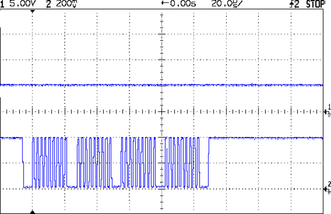
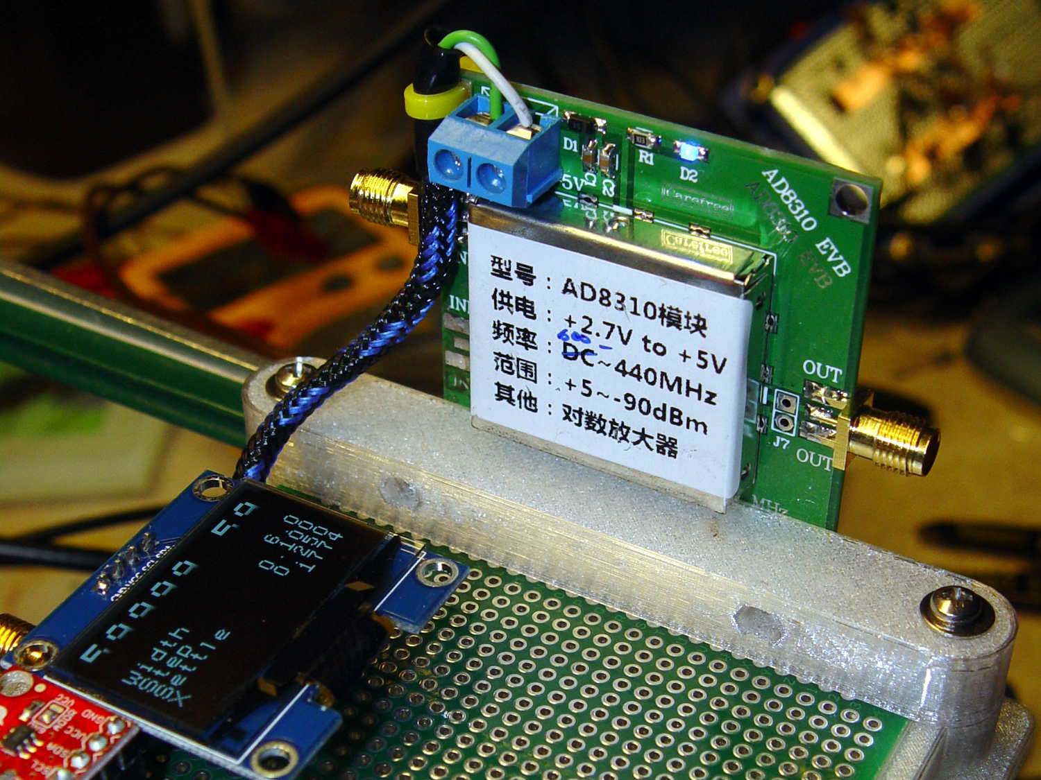
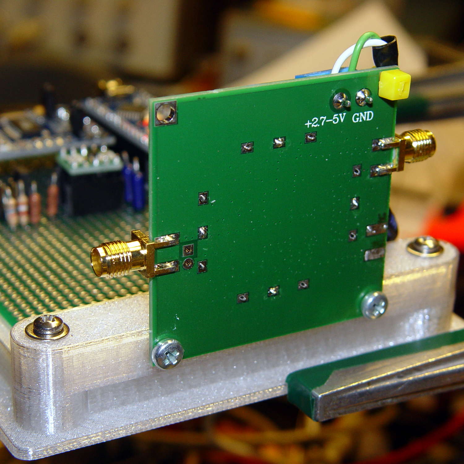
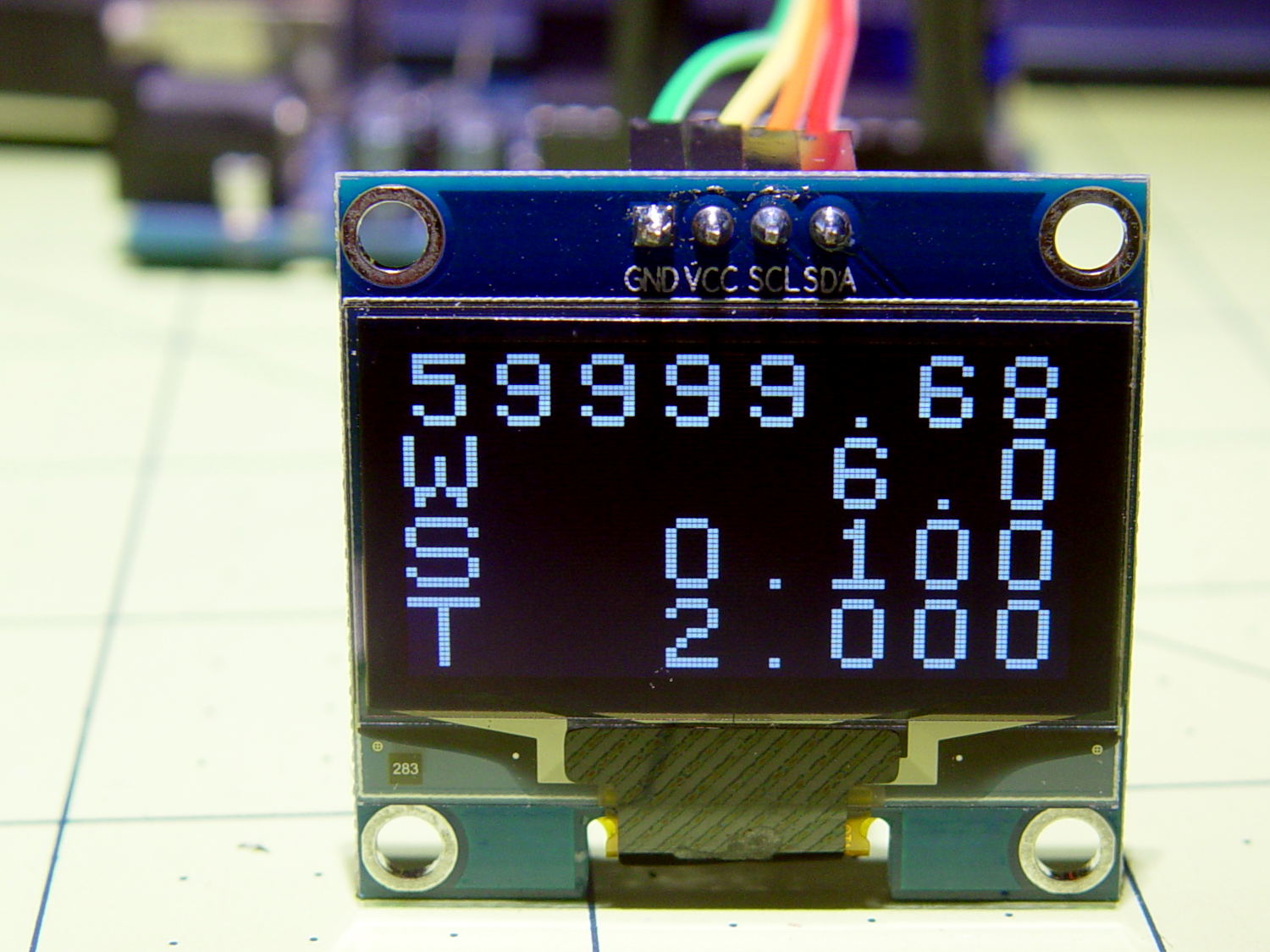
    // Test support frame for proto boards
    // Ed Nisley KE4ZNU – Jan 2017
    // June 2017 – Add side-mount bracket
    Layout = "Bracket";
    ClampFlange = true;
    Channel = false;
    //- Extrusion parameters – must match reality!
    ThreadThick = 0.25;
    ThreadWidth = 0.40;
    function IntegerMultiple(Size,Unit) = Unit * ceil(Size / Unit);
    Protrusion = 0.1;
    HoleWindage = 0.2;
    //- Screw sizes
    inch = 25.4;
    Tap4_40 = 0.089 * inch;
    Clear4_40 = 0.110 * inch;
    Head4_40 = 0.211 * inch;
    Head4_40Thick = 0.065 * inch;
    Nut4_40Dia = 0.228 * inch;
    Nut4_40Thick = 0.086 * inch;
    Washer4_40OD = 0.270 * inch;
    Washer4_40ID = 0.123 * inch;
    ID = 0;
    OD = 1;
    LENGTH = 2;
    Insert = [3.9,4.6,5.8];
    //- PCB sizes
    PCBSize = [80.0,120.0,1.6];
    PCBShelf = 1.5;
    Clearance = 2*[ThreadWidth,ThreadWidth,0];
    WallThick = 4.0;
    FrameHeight = 8.0;
    ScrewOffset = 0.0 + Clear4_40/2;
    ScrewSites = [[-1,1],[-1,1]]; // -1/0/+1 = left/mid/right and bottom/mid/top
    OAHeight = FrameHeight + Clearance[2] + PCBSize[2];
    echo(str("OAH: ",OAHeight));
    FlangeExtension = 3.0;
    FlangeThick = IntegerMultiple(2.0,ThreadThick);
    Flange = PCBSize
    + 2*[ScrewOffset,ScrewOffset,0]
    + 2*[Washer4_40OD,Washer4_40OD,0]
    + [2*FlangeExtension,2*FlangeExtension,(FlangeThick – PCBSize[2])]
    ;
    echo(str("Flange: ",Flange));
    NumSides = 4*5;
    WireChannel = [Flange[0],15.0,3.0 + PCBSize[2]];
    WireChannelOffset = [Flange[0]/2,25.0,(FrameHeight + PCBSize[2] – WireChannel[2]/2)];
    //- Adjust hole diameter to make the size come out right
    module PolyCyl(Dia,Height,ForceSides=0) { // based on nophead's polyholes
    Sides = (ForceSides != 0) ? ForceSides : (ceil(Dia) + 2);
    FixDia = Dia / cos(180/Sides);
    cylinder(r=(FixDia + HoleWindage)/2,h=Height,$fn=Sides);
    }
    //- Build things
    if (Layout == "Frame")
    difference() {
    union() { // body block
    translate([0,0,OAHeight/2])
    cube(PCBSize + Clearance + [2*WallThick,2*WallThick,FrameHeight],center=true);
    for (x=[-1,1], y=[-1,1]) { // screw bosses
    translate([x*(PCBSize[0]/2 + ScrewOffset),
    y*(PCBSize[1]/2 + ScrewOffset),
    0])
    cylinder(r=Washer4_40OD,h=OAHeight,$fn=NumSides);
    }
    if (ClampFlange) // flange for work holder
    linear_extrude(height=Flange[2])
    hull()
    for (i=[-1,1], j=[-1,1]) {
    translate([i*(Flange[0]/2 – Washer4_40OD/2),j*(Flange[1]/2 – Washer4_40OD/2)])
    circle(d=Washer4_40OD,$fn=NumSides);
    }
    }
    for (x=[-1,1], y=[-1,1]) { // screw position indexes
    translate([x*(PCBSize[0]/2 + ScrewOffset),
    y*(PCBSize[1]/2 + ScrewOffset),
    -Protrusion])
    rotate(x*y*180/(2*6))
    PolyCyl(Clear4_40,(OAHeight + 2*Protrusion),6); // screw clearance holes
    translate([x*(PCBSize[0]/2 + ScrewOffset),
    y*(PCBSize[1]/2 + ScrewOffset),
    OAHeight – PCBSize[2] – Insert[LENGTH]])
    rotate(x*y*180/(2*6))
    PolyCyl(Insert[OD],Insert[LENGTH] + Protrusion,6); // inserts
    translate([x*(PCBSize[0]/2 + ScrewOffset),
    y*(PCBSize[1]/2 + ScrewOffset),
    OAHeight – PCBSize[2]])
    PolyCyl(1.2*Washer4_40OD,(PCBSize[2] + Protrusion),NumSides); // washers
    }
    translate([0,0,OAHeight/2]) // through hole below PCB
    cube(PCBSize – 2*[PCBShelf,PCBShelf,0] + [0,0,2*OAHeight],center=true);
    translate([0,0,(OAHeight – (PCBSize[2] + Clearance[2])/2 + Protrusion/2)]) // PCB pocket on top
    cube(PCBSize + Clearance + [0,0,Protrusion],center=true);
    if (Channel)
    translate(WireChannelOffset) // opening for wires from bottom side
    cube(WireChannel + [0,0,Protrusion],center=true);
    }
    // Add-on bracket to hold smaller PCB upright at edge
    PCB2Insert = [3.0,4.9,4.1];
    PCB2OC = 45.0;
    if (Layout == "Bracket")
    difference() {
    hull() // frame body block
    for (x=[-1,1]) // bosses around screws
    translate([x*(PCBSize[0]/2 + ScrewOffset),0,0])
    cylinder(r=Washer4_40OD,h=OAHeight,$fn=NumSides);
    for (x=[-1,1]) // frame screw holes
    translate([x*(PCBSize[0]/2 + ScrewOffset),0,-Protrusion])
    rotate(x*180/(2*6))
    PolyCyl(Clear4_40,(OAHeight + 2*Protrusion),6);
    for (x=[-1,1]) // PCB insert holes
    translate([x*PCB2OC/2,(Washer4_40OD + Protrusion),OAHeight/2])
    rotate([90,0,0])
    cylinder(d=PCB2Insert[OD],h=2*(Washer4_40OD + Protrusion),$fn=6);
    }

  • AD9850 DDS Module: 1.3 inch I²C OLED FTW

    A white 1.3 inch I²C OLED turns out to be much more readable than the yellow-blue 0.96 inch version:

    Arduino with OLED - white 1.3 inch
    Arduino with OLED – white 1.3 inch

    Of course, after you make it readable, you immediately make room to cram more data on it:

    White 1.3 inch OLED on crystal tester
    White 1.3 inch OLED on crystal tester

    That’s on the proto board with the Arduino and AD9850 DDS ticking away on the left; the bright red MCP4725 DAC will eventually drive the scope’s X axis. Shifting the display to the I²C interface and cleaning up my SPI initialization code worked wonders: the DDS now steps a sine wave at 0.1 Hz (pretty nearly) intervals from 57.0 to 60.3 Hz.