The genuine Sony NP-BX1 that came with the AS30V camera suffers from voltage depression (green trace) and no longer survives a typical ride:
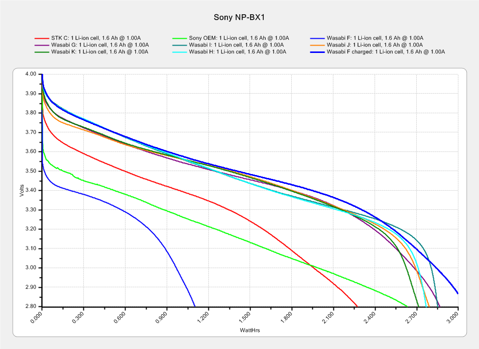
The STK C battery (red trace) is also pretty much kaput, so the two of them go into the recycle bag.
The very short blue trace is the Wasabi F battery after a ride, showing about 1 W·h remaining of the initial charge. After a full change, the upper blue trace shows it has a capacity in the same range as the others. Our rides are about an hour long, so the camera draws somewhat less than the 1 A test current, roughly what I’d estimated from other data.
The cluster of traces along the top show the remaining Wasabi batteries are all pretty much alike, with the older F and G batteries no worse than the newer (and unused) H I J K batteries. I’m underwhelmed by the overall performance of the latter four, as I’d expect them to be better than their well-used predecessors.
I’m still mulling an external 18650 cell grafted into a NP-BX1 carcass, but it’s stalled behind some other projects.