The Smell of Molten Projects in the Morning

Ed Nisley's Blog: Shop notes, electronics, firmware, machinery, 3D printing, laser cuttery, and curiosities. Contents: 100% human thinking, 0% AI slop.

Category: Electronics Workbench

Electrical & Electronic gadgets

  • Hall Effect LED Current Control: First Light

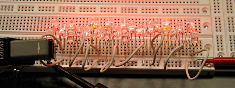
    This hideous proof-of-concept lashup gathers a bunch of stuff I’ve been investigating into what’s definitely in the running for the most over-the-top LED blinky light ever:
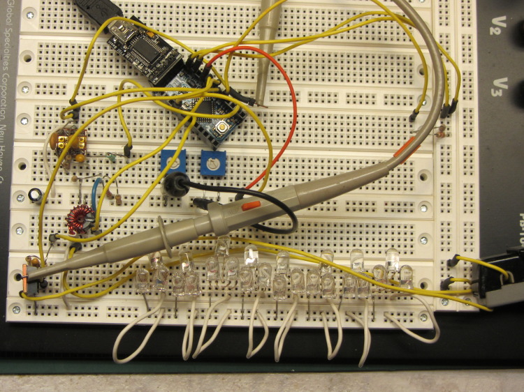
    Hall Effect LED Current Control - breadboard overview
    Hall Effect LED Current Control – breadboard overview

    The general idea:

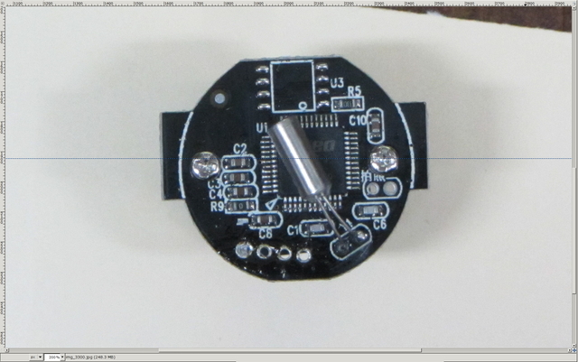
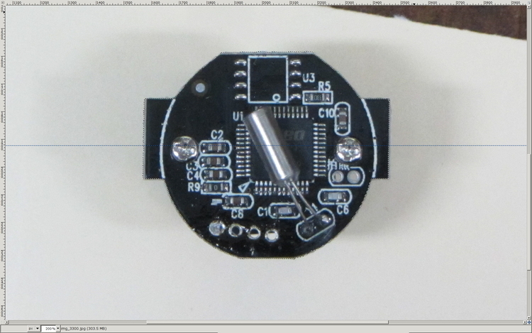
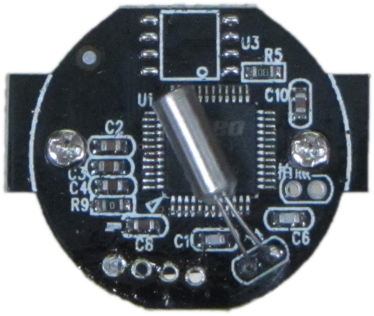
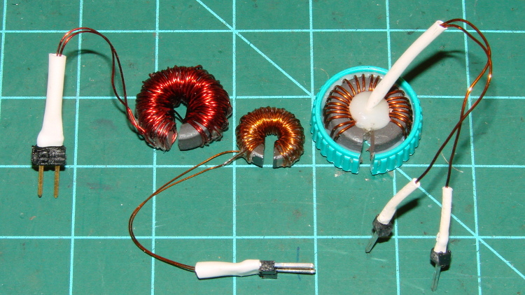
    A closer look at the key analog parts:

    Hall Effect LED Current Control - breadboard detail
    Hall Effect LED Current Control – breadboard detail

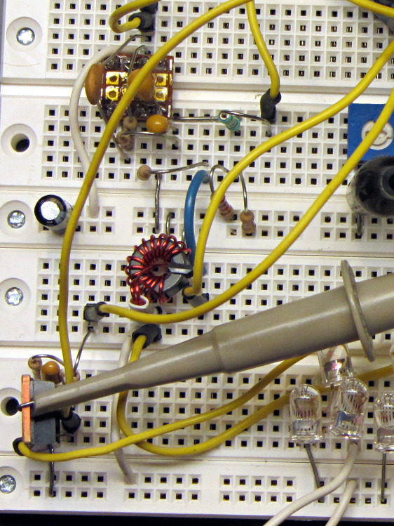
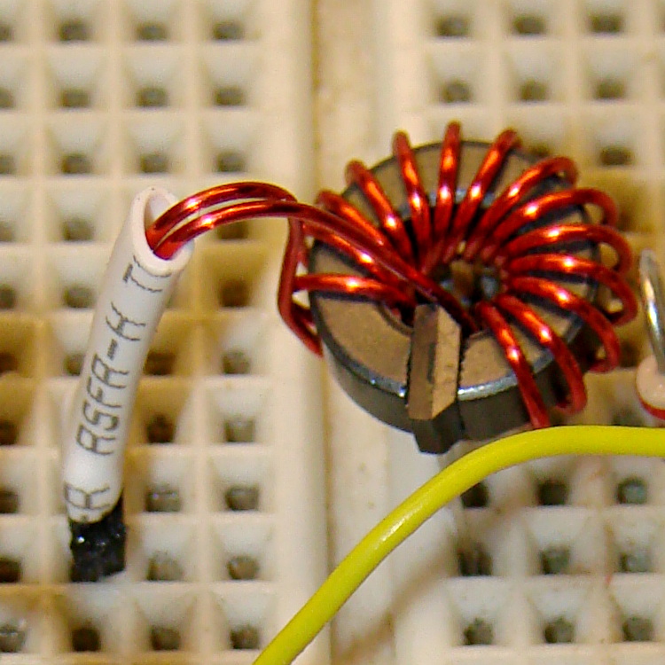
    The ferrite toroid near the middle surrounds that same “49E” Hall effect sensor. The ZVNL14 logic-level MOSFET in the lower right runs with about 2.4 V on the gate to put 120 mA through the LEDs. The cluster of parts just above it are the RC low-pass PWM filter, with the PWM running at 32 kHz. The snippet of perfboard near the top adapts a MAX4330 op amp to DIP pins. I used the twiddlepots to bring up the op amp and MOSFET circuitry by force-feeding bias and gate voltages.

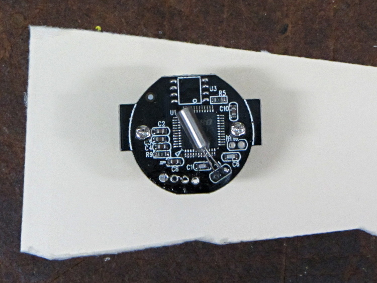
    The Arduino Pro Mini closes the feedback loop from current sensor to MOSFET gate. A knockoff Arduino Pro Mini is a $5 component, in onesies, delivered halfway around the planet. For low-volume stuff like this, you just build it right in and move on; there’s no reason to lay out a PCB with an ATmega328 chip and a handful of other parts. Unless you’re worried about power consumptions, as described below.

    The schematic:

    Hall Effect Current Feedback LED Driver - prototype schematic
    Hall Effect Current Feedback LED Driver – prototype schematic

    The MAX4330 removes the Hall effect sensor’s VCC/2 bias, but it turns out the offset varies by enough from part to part and over temperature that a single twiddlepot setting won’t suffice. The RC filter near the middle of the schematic converts an Arduino PWM output into a voltage between 2.0 and 3.0 V, which puts more PWM resolution where it matters; the default 0.4% PWM steps are just too coarse. I think 16 bit PWM resolution would be A Very Good Thing here.

    The first-pass program nulls the offset once, during the startup routine, but nulling whenever the LEDs turn off would be a Good Idea. The offset steps are 8 mV, about what you’d expect from 2/5 of the nominal 20 mV PWM increments. It ramps the offset up from zero, but you’d probably want to use a binary search.

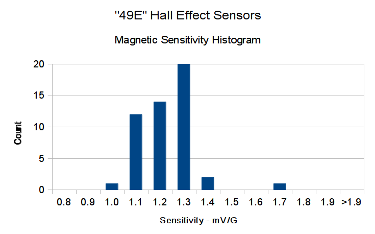
    The op amp has a voltage gain of about 28 that scales the toroid-plus-Hall-sensor output so that 500 mA in the winding produces 5 V. That gain isn’t quite high enough for the 120 mA I’m using for this collection of LEDs , but it makes the coefficient a nice round 0.10. It’d be good to have a calibrated current load, something around 100 mA, that would allow auto-calibration.

    A 50% voltage divider lets the Arduino measure the nominal 7.4 V battery voltage and decide when to lower the current or change the blink pattern or kvetch about imminent blackout or something. Knowing both the battery voltage and the resistance of the current calibration load would let the program calculate the actual current for calibration. Given two calibration loads, then you could derive both the gain and the remaining offset; that’s likely too much trouble.

    The Pro Mini board has a voltage regulator that provides +5 V for everything else in the circuit, which means putting the microcontroller into sleep mode won’t save any battery power. I think a p-channel MOSFET switch and a suicide output from the Arduino will be in order. A vibration sensor would give you auto power on and off, which would be a nice touch; MEMS sensors seem to want 3.3-ish V for supply and logic.

    The entire lashup runs at about 60 mA with the LEDs turned off, which is way too high and may include some breadboard screwups; considerable reduction will be in order before this circuit makes any sense. The Hall effect sensor costs about 4 mA all by itself, plus another milliamp in the load resistor. The microcontroller should be around 10 – 20 mA, but the datasheet makes some assumptions that aren’t true for the Arduino runtime.

    The program brute-forces the pulse timing, just to get this thing working. The main loop stalls while the LEDs are on, which is obviously a Bad Thing. The ADC conversions do some averaging, but I’m not confident it works well enough. The PWM output routine includes an entirely empirical delay to cover the filter time constants.

    The blink pattern should be in a table. Given linear current control, you can have variable brightness; a “night taillight” mode that isn’t so shatteringly bright would be a Good Idea. The table might contain gate voltages for each current level, updated during the last pulse, so that the output would be Pretty Close at the beginning; you’d measure those values during startup.

    A button or two for mode selection might be in order. Sealing buttons is always a problem, but this thing might not be totally waterproof anyway.

    But it blinks!

  • eBay “49E” Hall Effect Sensors: Parameter Spread

    A bag of 50 cheap Hall effect sensors arrived from the usual eBay vendor, who was different from all previous eBay vendors (if in name only). Passing 124 mA through the armored FT50 toroid with 25 turns of 26 AWG wire, we find this distribution of bias points, measured as the offset from the actual VCC/2:

    eBay 49E Hall Effect Sensor Bias Histogram
    eBay 49E Hall Effect Sensor Bias Histogram

    The bias point is actually referenced to the negative terminal (usually ground) with a ±0.25 V variation around the nominal. SS49 sensors run about 0.5 V below VCC/2 (2.25 V with a 5 V supply), SS49E sensors at 2.5 V with a tighter VCC limit that suggests you better stay pretty close to 5.0 V.

    Allowing for the fact that I really don’t have good control over the actual magnetic field, the gain distribution seems tight:

    eBay 49E Hall Effect Sensor Sensitivity Histogram
    eBay 49E Hall Effect Sensor Sensitivity Histogram

    You’ll recall the Genuine Honeywell sensor specs:

    • SS49 – nominal 0.9 mV/G, limits 0.6 to 1.25 mV/G
    • SS49E – nominal 1.4 mV/G, limits 1.0 to 1.75 mV/G

    The gain is roughly half that of the previous “49E” sensors, confirmed by sticking one of them this field. I don’t know which is more accurate, but these have a much prettier distribution.

    So this lot resembles 49E sensors in both bias and gain.

    Given the bias variation, though, it’s obvious that a DC application must measure the zero-field output and apply an analog offset to the amplifier, because a twiddlepot setting won’t suffice. Most likely, you’d want to update the offset every now and again to compensate for temperature variation, too.

    Tossing the outliers gives an average gain of 1.17, which would give results within 10% over the lot. Given that you don’t care about the actual magnetic field, you could calibrate the output voltage for a known input current and get really nice results.

    If you were doing position sensing from a known magnet, you’d want better control of the magnetic field gradient.

  • Series-Parallel LED Current

    The collection of LEDs that I’ve been abusing with 100 mA pulses at 20% duty cycle got lined up in parallel, with three LEDs in series, driven from a bench power supply set to limit the current to about 180 mA:

    Series-parallel LED test fixture
    Series-parallel LED test fixture

    I sweetened the mix by adding a few other LEDs that had served their time in hell, then took some data by clipping the Tek Hall effect current probe around each of the white wires in turn:

    Color LED1 LED2 LED3 Divisions Current – mA Total voltage
    Red 1.98 1.98 1.94 4.7 23.5 5.90
    Red 1.95 1.95 2.00 3.4 17.0 5.90
    Red 1.97 1.97 1.97 5.1 25.5 5.91
    Yellow 1.97 1.97 1.96 4.5 22.5 5.90
    Yellow 1.97 1.96 1.97 4.6 23.0 5.90
    Red 1.98 1.98 1.94 4.6 23.0 5.90
    Red 1.95 1.95 2.00 3.3 16.5 5.90
    Red (new!) 1.99 1.96 1.94 6.4 32.0 5.89

    Despite the decimals, don’t trust anything beyond the first two digits.

    The LEDs started out with 6.03 V across them at that current, then settled down to 5.92 V after a few minutes of warming up.

    The “new” Red string replaces a trio of old LEDs incinerated by a DVM probe fumble. They have a much higher current at the same voltage; the older LEDs have been abused enough to pass a lower current.

    As an experiment, I swapped the LED with the 2.00 V drop in the string with the lowest current (line 7) and the LED with the 1.94 V drop in a string with higher current (line 6), only to find that the current followed the LEDs. Evidently, those LEDs were the limiting factor, even though their forward drops weren’t the same in their new strings.

    So it seems binning based on forward drop doesn’t help much. Perhaps just line up a bunch of three-LED strings (forcing all of them to see the same forward drop), measure their current, and reject the highest and lowest strings to get a decent match among the remainder?

  • Measuring Objects for 3D Modeling: USB Video Camera

    A brace of “Fashion” USB video cameras arrived from halfway around the planet. According to the eBay description and the legend around the lens, they’re “5.0 Megapixel”:

    Fashion USB camera - case front
    Fashion USB camera – case front

    The reality, of course, is that for five bucks delivered you get 640×480 VGA resolution at the hardware level and their Windows driver interpolates the other 4.7 megapixels. VGA resolution will be good enough for my simple needs, particularly because the lens has a mechanical focus adjustment; the double-headed arrow symbolizes the focus action.

    But the case seemed entirely too bulky and awkward. A few minutes with a #0 Philips screwdriver extracted the actual camera hardware, which turns out to be a double-sided PCB with a lens assembly on the front:

    Fashion USB video - case vs camera
    Fashion USB video – case vs camera

    The PCB has asymmetric tabs that ensure correct orientation in the case:

    Fashion USB camera - wired PCB rear
    Fashion USB camera – wired PCB rear

    In order to build an OpenSCAD model for a more compact case, we need the dimensions of that PCB and those tabs…

    Start with a picture of the back of the PCB against white paper, taken from a few feet to flatten the perspective:

    img_3300 - Camera PCB on white paper
    img_3300 – Camera PCB on white paper

    Load it into The GIMP, zoom in, and pull a horizontal guide line down to about the middle of the image:

    Camera PCB - horizontal guide - scaled
    Camera PCB – horizontal guide – scaled

    Rotate to align the two screws horizontally (they need not be centered on the guide, just lined up horizontally):

    Camera PCB - rotated to match horizontal guide - scaled
    Camera PCB – rotated to match horizontal guide – scaled

    Use the Magic Scissors to select the PCB border (it’s the nearly invisible ragged dotted outline):

    Camera PCB - scissors selection - scaled
    Camera PCB – scissors selection – scaled

    Flip to Quick Mask mode and clean up the selection as needed:

    Camera PCB - quick mask cleanup - scaled
    Camera PCB – quick mask cleanup – scaled

    Flip back to normal view, invert the selection (to select the background, not the PCB), and delete the background to isolate the PCB:

    Camera PCB - isolated - scaled
    Camera PCB – isolated – scaled

    Tight-crop the PCB and flatten the image to get a white background:

    Camera PCB - isolated - scaled
    Camera PCB – isolated – scaled

    Fetch some digital graph paper from your favorite online source. The Multi-color (Light Blue / Light Blue / Light Grey) Multi-weight (1.0×0.6×0.3 pt) grid (1 / 2 / 10) works best for me, but do what you like. Get a full Letter / A4 size sheet, because it’ll come in handy for other projects.

    Open it up (converting at 300 dpi), turn it into a layer atop the PCB image, use the color-select tool to select the white background between the grid lines, then delete the selection to leave just the grid with transparency:

    Camera PCB with grid overlay - unscaled
    Camera PCB with grid overlay – unscaled

    We want one minor grid square to be 1×1 mm on the PCB image, sooo…

    • Accurately measure a large feature on the real physical object: 27.2 mm across the tabs
    • Drag the grid to align a major line with one edge of the PCB
    • Count the number of minor square across to the other side of the image: 29.5
    • Scale the grid overlay layer by image/physical size: 1.085 = 29.5/27.2
    • Drag the grid so it’s neatly centered on the object (or has a major grid intersection somewhere useful)

    That produces a calibrated overlay:

    Camera PCB with grid overlay
    Camera PCB with grid overlay

    Then it’s just a matter of reading off the coordinates, with each minor grid square representing 1.0 mm in the real world, and writing some OpenSCAD code…

  • SMD-to-DIP Adapter: Pin Soldering “Fixture”

    I needed a rail-to-rail op amp in a DIP package to breadboard the amplifier for those toroids and came up dry, so I sawed out a protoboard square, glued a MAX4330 in SOT23-5 atop it in classic dead-bug style, rearranged the leads into the standard DIP pinout, and moved on:

    MAX4330 dead-bug style on DIP adapter
    MAX4330 dead-bug style on DIP adapter

    The trick to getting the header pins aligned is to stick ’em in a pile of perfboards, which instantly makes them stand up straight and parallel:

    img_3430 - SMD-to-DIP adapter - PCB soldering fixture
    img_3430 – SMD-to-DIP adapter – PCB soldering fixture

    Stick the square adapter atop the headers, solder all eight pins, glue down the SOT23, and solder it with wire-wrap snippets. Ugly, but workable…

  • Air-gapped Ferrite Toroid Data

    For an upcoming Circuit Cellar column on Hall effect current sensing, I slit another pair of toroids:

    Slitting FT37 ferrite toroid
    Slitting FT37 ferrite toroid

    Then wound them with grossly excessive amounts of wire (the up-armored core on the right appeared earlier):

    Slit Ferrite Toroid current sensors
    Slit Ferrite Toroid current sensors

    The smaller toroid is an FT37-43 that barely covers the active area of an SS49-style Hall effect sensor, but experience with the FT50 toroid suggests that’ll be entirely enough:

    slit FT37 toroid trial fit to SS48-style Hall effect sensor
    slit FT37 toroid trial fit to SS48-style Hall effect sensor

    Data on the uncut toroids:

    Property FT50-61 FT37-43
    Outer diameter (OD) – inch 0.50 0.375
    Inner diameter (ID) – inch 0.281 0.187
    Length – inch 0.188 0.125
    Cross section area – cm2 0.133 0.133
    Mean path length (MPL) – cm 3.02 2.15
    Volume – cm3 0.401 0.163
    Relative Permeability (μr ) 125 850
    Saturation flux G @ 10 Oe 2350 2750
    Inductance factor (AL) – nH/turn2 68.0 420

    Those overstuffed windings improved the sensitivity, but increased the winding resistance far beyond what’s reasonable.

    Data on the slit toroids:

    Toroid ID FT50-61 FT37-43 FT50-61
    Measured air gap – cm 0.15 0.15 0.17
    Winding data
    Turns 120 80 25
    Wire gauge – AWG 28 32 26
    Winding resistance – mΩ 530 920 100
    Predicted B field – G/A 872 660 163
    Hall effect sensor @ 1.9 mV/G
    Predicted output – mV/mA 1.7 1.3 0.31
    Actual output – mV/mA 1.9 1.9 0.37
    Actual/predicted ratio – % +12 +46 +19

    The last few lines in that table show the transimpedance (transresistance, really, but …) based on the winding current to Hall sensor output voltage ratio (in either mV/mA or V/A, both dimensionally equivalent to ohms), which is why the toroid’s internal magnetic flux doesn’t matter as long as it’s well below saturation.

    Gnawing the 80 turn winding off the FT37-43 toroid and rewinding it with 15 turns of 24 AWG wire dropped the winding resistance to 23 mΩ and the transimpedance to 0.36 mV/mA:

    FT37-43 with 15 turns 24 AWG - Hall sensor
    FT37-43 with 15 turns 24 AWG – Hall sensor

    However, applying a voltage gain of about 28 (after removing the sensor’s VCC/2 bias) will produce a 0-to-5 V output from 500 mA input, which seems reasonable.

  • Wouxun KG-UV3D Batteries: Age and Cycle Effects

    The first Wouxun (evidently pronounced “ocean”) KG-UV3D HT spent a month or two in my bike, lashed to a kludged version of the APRS+voice interface box and powered by its own lithium-ion pack. After I got the circuit worked out and built a duplicate, I picked up a second HT for Mary’s bike; as a result, that battery pack never got much use.

    A pair of discharge tests shows the difference:

    Wouxun 7.4 V Packs
    Wouxun 7.4 V Packs

    The 2011-03 battery has almost exactly the rated 1.7 A·h capacity, at least if you’re willing to run it down to 6 V, and the 2012-06 pack delivers 1.9 A·h. Electronic gadgets measure state-of-charge using the battery voltage, so the older pack “looks” like it has much less capacity: it runs about 100 mV lower than the newer pack out to 1.2 A·h, then falls off the cliff. Looks to me like one of the two cells inside is fading faster than the other; so it goes.

    I’m still thinking of using these to power some LED taillights, because they have a nice form factor and built-in latches:

    Wouxun KG-UV3D - battery pack latch
    Wouxun KG-UV3D – battery pack latch