Those little OLED displays might just work:

The U8X8 driver produces those double-size bitmap characters; the default 8×8 matrix seem pretty much unreadable on a 0.96 inch OLED at any practical distance from a benchtop instrument. They might be workable on a 1.3 inch white OLED, minus the attractive yellow highlight for the frequency in the top line.
The OLED uses an SPI interface, although the U8X8 library clobbers my (simpleminded) SPI configuration for the AD9850 DDS and I’ve dummied out the DDS outputs. A soon-to-arrive I²C OLED should resolve that problem; changing the interface from SPI to I²C involves changing the single line of code constructing the driver object, so It Should Just Work.
The U8X8 driver writes directly to the display, thus eliminating the need for a backing buffer in the Arduino’s painfully limited RAM. I think the library hauls in all possible fonts to support font selection at runtime, even though I need at most two fonts, so it may be worthwhile to hack the unneeded ones from the library (or figure out if I misunderstand the situation and the Flash image includes only the fonts actually used). Each font occupies anywhere from 200 to 2000 bytes, which I’d rather have available for program code. Chopping out unused functions would certainly be less useful.
The display formatting is a crude hack just to see what the numbers look like:
    int ln = 0;
    u8x8.draw2x2String(0,ln,Buffer);
    ln += 2;

    TestFreq.fx_64 = ScanTo.fx_64 - ScanFrom.fx_64;
    PrintFixedPtRounded(Buffer,TestFreq,1);
    u8x8.draw2x2String(0,ln,"W       ");
    u8x8.draw2x2String(2*(8-strlen(Buffer)),ln,Buffer);
    ln += 2;

    PrintFixedPtRounded(Buffer,ScanStep,3);
    u8x8.draw2x2String(0,ln,"S       ");
    u8x8.draw2x2String(2*(8-strlen(Buffer)),ln,Buffer);
    ln += 2;

    TestFreq.fx_32.high = SCAN_SETTLE;                    // milliseconds
    TestFreq.fx_32.low = 0;
    TestFreq.fx_64 /= KILO;                               // to seconds
    PrintFixedPtRounded(Buffer,TestFreq,3);
    u8x8.draw2x2String(0,ln,"T       ");
    u8x8.draw2x2String(2*(8-strlen(Buffer)),ln,Buffer);
    ln += 2;
Updating the display produces a noticeable and annoying flicker, which isn’t too surprising, so each value should have an “update me” flag to avoid gratuitous writes. Abstracting the display formatting into a table-driven routine might be appropriate, when I need more than one layout, but sheesh.
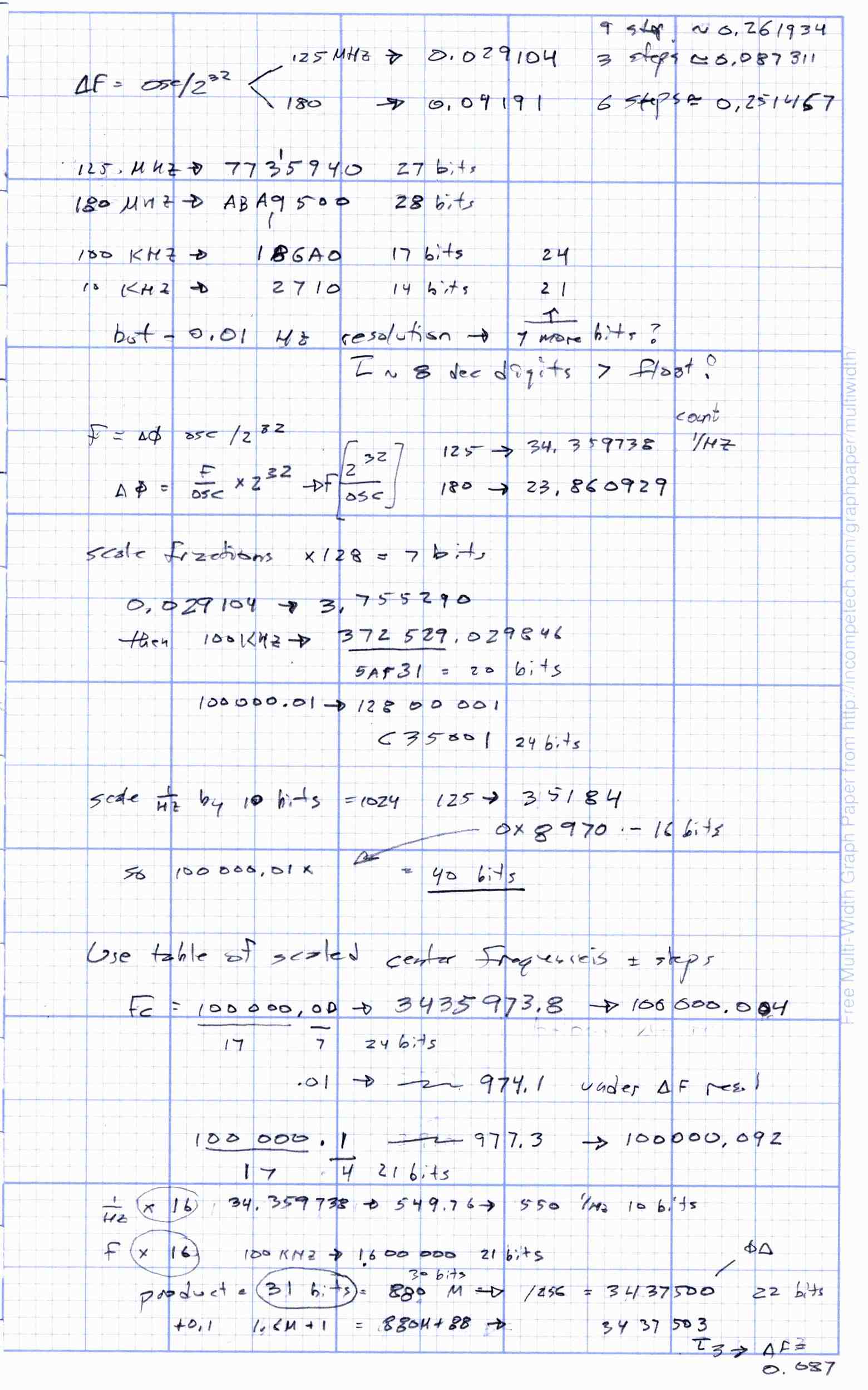
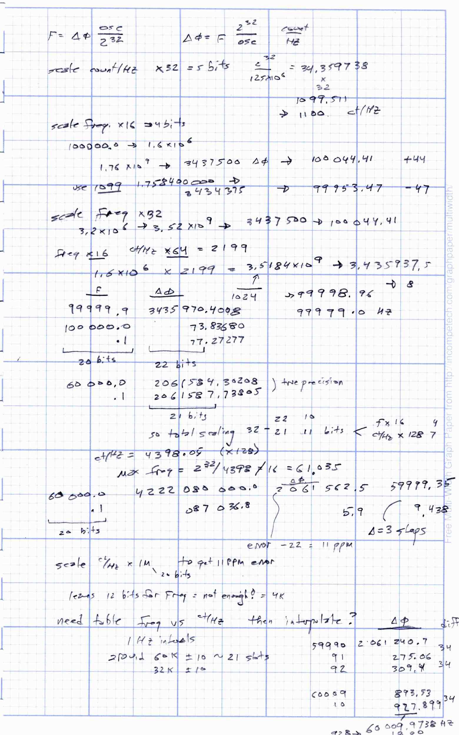
I calculate the actual frequency from the 32 bit integer delta phase word written to the DDS, rather than use the achingly precise fixed point value, so a tidy 0.100 Hz frequency step doesn’t produce neat results. Instead, the displayed value will be within ±0.0291 Hz (the frequency resolution) of the desired frequency, which probably makes more sense for the very narrow bandwidths involved in a quartz crystal test gadget.
Computing the frequency step size makes heavy use of 64 bit integers:
//  ScanStep.fx_64 = One.fx_64 / 4;                       // 0.25 Hz = 8 or 9 tuning register steps
  ScanStep.fx_64 = One.fx_64 / 10;                    // 0.1 Hz = 3 or 4 tuning register steps
//  ScanStep.fx_64 = One.fx_64 / 20;                    // 0.05 Hz = 2 or 3 tuning register steps
//  ScanStep = HzPerCt;                                   // smallest possible frequency step
The fixed point numbers resulting from those divisions will be accurate to nine decimal places; good enough for what I need.
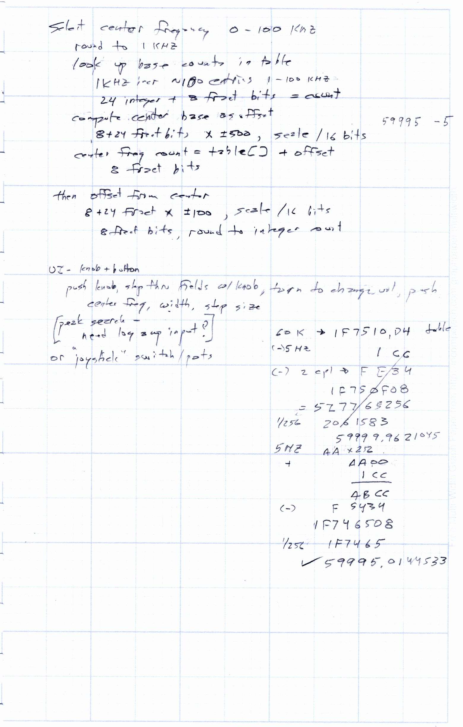
The sensible way of handling discrete scan width / step size / settling time options is through menus showing the allowed choices, with joystick / joyswitch navigation & selection, rather than keyboard entry. An analog joystick has the distinct advantage of using two analog inputs, not four digital pins, although the U8X8 driver includes a switch-driven menu handler.
There’s a definite need to log all the values through the serial output for data collection without hand transcription.
The Arduino source code as a GitHub Gist:
| // OLED display test for 60 kHz crystal tester | |
| #include <avr/pgmspace.h> | |
| //#include <SPI.h> | |
| #include <U8g2lib.h> | |
| #include <U8x8lib.h> | |
| // Turn off DDS SPI for display checkout | |
| #define DOSPI 0 | |
| //——————— | |
| // Pin locations | |
| // SPI uses hardware support: those pins are predetermined | |
| #define PIN_HEARTBEAT 9 | |
| #define PIN_DDS_RESET 7 | |
| #define PIN_DDS_LATCH 8 | |
| #define PIN_DISP_SEL 4 | |
| #define PIN_DISP_DC 5 | |
| #define PIN_DISP_RST 6 | |
| #define PIN_SCK 13 | |
| #define PIN_MISO 12 | |
| #define PIN_MOSI 11 | |
| #define PIN_SS 10 | |
| char Buffer[10+1+10+1]; // string buffer for long long conversions | |
| #define GIGA 1000000000LL | |
| #define MEGA 1000000LL | |
| #define KILO 1000LL | |
| struct ll_fx { | |
| uint32_t low; // fractional part | |
| uint32_t high; // integer part | |
| }; | |
| union ll_u { | |
| uint64_t fx_64; | |
| struct ll_fx fx_32; | |
| }; | |
| union ll_u CtPerHz; // will be 2^32 / 125 MHz | |
| union ll_u HzPerCt; // will be 125 MHz / 2^32 | |
| union ll_u One; // 1.0 as fixed point | |
| union ll_u Tenth; // 0.1 as fixed point | |
| union ll_u TenthHzCt; // 0.1 Hz in counts | |
| // All nominal values are integers for simplicity | |
| #define OSC_NOMINAL (125 * MEGA) | |
| #define OSC_OFFSET_NOMINAL (-344LL) | |
| union ll_u OscillatorNominal; // nominal oscillator frequency | |
| union ll_u OscOffset; // … and offset, which will be signed 64-bit value | |
| union ll_u Oscillator; // true oscillator frequency with offset | |
| union ll_u CenterFreq; // center of scan width | |
| #define SCAN_WIDTH 6 | |
| #define SCAN_SETTLE 2000 | |
| union ll_u ScanFrom, ScanTo, ScanFreq, ScanStep; // frequency scan settings | |
| uint8_t ScanStepCounter; | |
| union ll_u TestFreq,TestCount; // useful variables | |
| //U8X8_SH1106_128X64_NONAME_4W_HW_SPI u8x8(PIN_DISP_SEL, PIN_DISP_DC , PIN_DISP_RST); | |
| U8X8_SH1106_128X64_NONAME_4W_SW_SPI u8x8(PIN_SCK, PIN_MOSI, PIN_DISP_SEL, PIN_DISP_DC , PIN_DISP_RST); | |
| //U8X8_SH1106_128X64_NONAME_HW_I2C u8x8(U8X8_PIN_NONE); | |
| #define HEARTBEAT_MS 3000 | |
| unsigned long MillisNow,MillisThen; | |
| //———– | |
| // Useful functions | |
| // Pin twiddling | |
| void TogglePin(char bitpin) { | |
| digitalWrite(bitpin,!digitalRead(bitpin)); // toggle the bit based on previous output | |
| } | |
| void PulsePin(char bitpin) { | |
| TogglePin(bitpin); | |
| TogglePin(bitpin); | |
| } | |
| // SPI I/O | |
| void EnableSPI(void) { | |
| digitalWrite(PIN_SS,HIGH); // set SPI into Master mode | |
| SPCR |= 1 << SPE; | |
| } | |
| void DisableSPI(void) { | |
| SPCR &= ~(1 << SPE); | |
| } | |
| void WaitSPIF(void) { | |
| while (! (SPSR & (1 << SPIF))) { | |
| TogglePin(PIN_HEARTBEAT); | |
| TogglePin(PIN_HEARTBEAT); | |
| continue; | |
| } | |
| } | |
| byte SendRecSPI(byte Dbyte) { // send one byte, get another in exchange | |
| SPDR = Dbyte; | |
| WaitSPIF(); | |
| return SPDR; // SPIF will be cleared | |
| } | |
| // DDS module | |
| void EnableDDS(void) { | |
| digitalWrite(PIN_DDS_LATCH,LOW); // ensure proper startup | |
| digitalWrite(PIN_DDS_RESET,HIGH); // minimum reset pulse 40 ns, not a problem | |
| digitalWrite(PIN_DDS_RESET,LOW); | |
| delayMicroseconds(1); // max latency 100 ns, not a problem | |
| DisableSPI(); // allow manual control of outputs | |
| digitalWrite(PIN_SCK,LOW); // ensure clean SCK pulse | |
| PulsePin(PIN_SCK); // … to latch hardwired config bits | |
| PulsePin(PIN_DDS_LATCH); // load hardwired config bits = begin serial mode | |
| EnableSPI(); // turn on hardware SPI controls | |
| SendRecSPI(0x00); // shift in serial config bits | |
| PulsePin(PIN_DDS_LATCH); // load serial config bits | |
| } | |
| // Write delta phase count to DDS | |
| // This comes from the integer part of a 64-bit scaled value | |
| void WriteDDS(uint32_t DeltaPhase) { | |
| SendRecSPI((byte)DeltaPhase); // low-order byte first | |
| SendRecSPI((byte)(DeltaPhase >> 8)); | |
| SendRecSPI((byte)(DeltaPhase >> 16)); | |
| SendRecSPI((byte)(DeltaPhase >> 24)); | |
| SendRecSPI(0x00); // 5 MSBs = phase = 0, 3 LSBs must be zero | |
| PulsePin(PIN_DDS_LATCH); // write data to DDS | |
| } | |
| //———– | |
| // Round scaled fixed point to specific number of decimal places: 0 through 8 | |
| // You should display the value with only Decimals characters beyond the point | |
| // Must calculate rounding value as separate variable to avoid mystery error | |
| uint64_t RoundFixedPt(union ll_u TheNumber,unsigned Decimals) { | |
| union ll_u Rnd; | |
| Rnd.fx_64 = (One.fx_64 / 2) / (pow(10LL,Decimals)); | |
| TheNumber.fx_64 = TheNumber.fx_64 + Rnd.fx_64; | |
| return TheNumber.fx_64; | |
| } | |
| //———– | |
| // Multiply two unsigned scaled fixed point numbers without overflowing a 64 bit value | |
| // The product of the two integer parts mut be < 2^32 | |
| uint64_t MultiplyFixedPt(union ll_u Mcand, union ll_u Mplier) { | |
| union ll_u Result; | |
| Result.fx_64 = ((uint64_t)Mcand.fx_32.high * (uint64_t)Mplier.fx_32.high) << 32; // integer parts (clear fract) | |
| Result.fx_64 += ((uint64_t)Mcand.fx_32.low * (uint64_t)Mplier.fx_32.low) >> 32; // fraction parts (always < 1) | |
| Result.fx_64 += (uint64_t)Mcand.fx_32.high * (uint64_t)Mplier.fx_32.low; // cross products | |
| Result.fx_64 += (uint64_t)Mcand.fx_32.low * (uint64_t)Mplier.fx_32.high; | |
| return Result.fx_64; | |
| } | |
| //———– | |
| // Long long print-to-buffer helpers | |
| // Assumes little-Endian layout | |
| void PrintHexLL(char *pBuffer,union ll_u FixedPt) { | |
| sprintf(pBuffer,"%08lx %08lx",FixedPt.fx_32.high,FixedPt.fx_32.low); | |
| } | |
| // converts all 9 decimal digits of fraction, which should suffice | |
| void PrintFractionLL(char *pBuffer,union ll_u FixedPt) { | |
| union ll_u Fraction; | |
| Fraction.fx_64 = FixedPt.fx_32.low; // copy 32 fraction bits, high order = 0 | |
| Fraction.fx_64 *= GIGA; // times 10^9 for conversion | |
| Fraction.fx_64 >>= 32; // align integer part in low long | |
| sprintf(pBuffer,"%09lu",Fraction.fx_32.low); // convert low long to decimal | |
| } | |
| void PrintIntegerLL(char *pBuffer,union ll_u FixedPt) { | |
| sprintf(pBuffer,"%lu",FixedPt.fx_32.high); | |
| } | |
| void PrintFixedPt(char *pBuffer,union ll_u FixedPt) { | |
| PrintIntegerLL(pBuffer,FixedPt); // do the integer part | |
| pBuffer += strlen(pBuffer); // aim pointer beyond integer | |
| *pBuffer++ = '.'; // drop in the decimal point, tick pointer | |
| PrintFractionLL(pBuffer,FixedPt); | |
| } | |
| void PrintFixedPtRounded(char *pBuffer,union ll_u FixedPt,unsigned Decimals) { | |
| char *pDecPt; | |
| FixedPt.fx_64 = RoundFixedPt(FixedPt,Decimals); | |
| PrintIntegerLL(pBuffer,FixedPt); // do the integer part | |
| pBuffer += strlen(pBuffer); // aim pointer beyond integer | |
| pDecPt = pBuffer; // save the point location | |
| *pBuffer++ = '.'; // drop in the decimal point, tick pointer | |
| PrintFractionLL(pBuffer,FixedPt); // do the fraction | |
| if (Decimals == 0) | |
| *pDecPt = 0; // 0 places means discard the decimal point | |
| else | |
| *(pDecPt + Decimals + 1) = 0; // truncate string to leave . and Decimals chars | |
| } | |
| //———– | |
| // Calculate useful "constants" from oscillator info | |
| // Args are integer constants in Hz | |
| void CalcOscillator(uint32_t Base,uint32_t Offset) { | |
| union ll_u Temp; | |
| Oscillator.fx_32.high = Base + Offset; // get true osc frequency from integers | |
| Oscillator.fx_32.low = 0; | |
| HzPerCt.fx_32.low = Oscillator.fx_32.high; // divide oscillator by 2^32 with simple shifting | |
| HzPerCt.fx_32.high = 0; | |
| CtPerHz.fx_64 = -1; // Compute (2^32 – 1) / oscillator | |
| CtPerHz.fx_64 /= (uint64_t)Oscillator.fx_32.high; // remove 2^32 scale factor from divisor | |
| TenthHzCt.fx_64 = MultiplyFixedPt(Tenth,CtPerHz); // 0.1 Hz as delta-phase count | |
| #if 0 | |
| printf("Inputs: %ld = %ld%+ld\n",Base+Offset,Base,Offset); | |
| PrintFixedPt(Buffer,Oscillator); | |
| printf("Osc freq: %s\n",Buffer); | |
| PrintFixedPt(Buffer,HzPerCt); | |
| printf("Hz/Ct: %s\n",Buffer); | |
| PrintFixedPt(Buffer,CtPerHz); | |
| printf("Ct/Hz: %s\n",Buffer); | |
| PrintFixedPt(Buffer,TenthHzCt); | |
| printf("0.1 Hz Ct: %s",Buffer); | |
| #endif | |
| } | |
| //– Helper routine for printf() | |
| int s_putc(char c, FILE *t) { | |
| Serial.write(c); | |
| } | |
| //———– | |
| void setup () | |
| { | |
| pinMode(PIN_HEARTBEAT,OUTPUT); | |
| digitalWrite(PIN_HEARTBEAT,HIGH); // show we got here | |
| Serial.begin (115200); | |
| fdevopen(&s_putc,0); // set up serial output for printf() | |
| Serial.println (F("DDS OLED exercise")); | |
| Serial.println (F("Ed Nisley – KE4ZNU – May 2017\n")); | |
| // DDS module controls | |
| pinMode(PIN_DDS_LATCH,OUTPUT); | |
| digitalWrite(PIN_DDS_LATCH,LOW); | |
| pinMode(PIN_DDS_RESET,OUTPUT); | |
| digitalWrite(PIN_DDS_RESET,HIGH); | |
| // Light up the display | |
| Serial.println("Initialize OLED"); | |
| u8x8.begin(); | |
| u8x8.setPowerSave(0); | |
| u8x8.setFont(u8x8_font_pxplusibmcga_f); | |
| u8x8.draw2x2String(0,0,"OLEDTest"); | |
| u8x8.drawString(0,2,"Ed Nisley"); | |
| u8x8.drawString(0,3," KE4ZNU"); | |
| u8x8.drawString(0,4,"May 2017"); | |
| // configure SPI hardware | |
| #if DOSPI | |
| SPCR = B01110001; // Auto SPI: no int, enable, LSB first, master, + edge, leading, f/16 | |
| SPSR = B00000000; // not double data rate | |
| pinMode(PIN_SS,OUTPUT); | |
| digitalWrite(PIN_SCK,HIGH); | |
| pinMode(PIN_SCK,OUTPUT); | |
| digitalWrite(PIN_SCK,LOW); | |
| pinMode(PIN_MOSI,OUTPUT); | |
| digitalWrite(PIN_MOSI,LOW); | |
| pinMode(PIN_MISO,INPUT_PULLUP); | |
| #endif | |
| TogglePin(PIN_HEARTBEAT); // show we got here | |
| // Calculate useful constants | |
| One.fx_64 = 1LL << 32; // Set up 1.0, a very useful constant | |
| Tenth.fx_64 = One.fx_64 / 10; // Likewise, 0.1 | |
| // Set oscillator "constants" | |
| CalcOscillator(OSC_NOMINAL,OSC_OFFSET_NOMINAL); | |
| TogglePin(PIN_HEARTBEAT); // show we got here | |
| // Set the crystal-under-test nominal frequency | |
| CenterFreq.fx_64 = One.fx_64 * (60 * KILO); | |
| #if 1 | |
| PrintFixedPtRounded(Buffer,CenterFreq,1); | |
| printf("Center: %s\n",Buffer); | |
| #endif | |
| // Set up scan limits based on center frequency | |
| ScanFrom.fx_64 = CenterFreq.fx_64 – SCAN_WIDTH * (One.fx_64 >> 1); | |
| ScanTo.fx_64 = CenterFreq.fx_64 + SCAN_WIDTH * (One.fx_64 >> 1); | |
| ScanFreq = ScanFrom; // start scan at lower limit | |
| // ScanStep.fx_64 = One.fx_64 / 4; // 0.25 Hz = 8 or 9 tuning register steps | |
| ScanStep.fx_64 = One.fx_64 / 10; // 0.1 Hz = 3 or 4 tuning register steps | |
| // ScanStep.fx_64 = One.fx_64 / 20; // 0.05 Hz = 2 or 3 tuning register steps | |
| // ScanStep = HzPerCt; // smallest possible frequency step | |
| #if 1 | |
| Serial.println("\nScan limits"); | |
| PrintFixedPtRounded(Buffer,ScanFrom,1); | |
| printf(" from: %11s\n",Buffer); | |
| PrintFixedPtRounded(Buffer,ScanFreq,1); | |
| printf(" at: %11s\n",Buffer); | |
| PrintFixedPtRounded(Buffer,ScanTo,1); | |
| printf(" to: %11s\n",Buffer); | |
| PrintFixedPtRounded(Buffer,ScanStep,3); | |
| printf(" step: %s\n",Buffer); | |
| #endif | |
| // Wake up and load the DDS | |
| #if DOSPI | |
| TestCount.fx_64 = MultiplyFixedPt(ScanFreq,CtPerHz); | |
| EnableDDS(); | |
| WriteDDS(TestCount.fx_32.high); | |
| #endif | |
| delay(2000); | |
| u8x8.clearDisplay(); | |
| u8x8.setFont(u8x8_font_artossans8_r); | |
| Serial.println("\nStartup done!"); | |
| MillisThen = millis(); | |
| } | |
| //———– | |
| void loop () { | |
| MillisNow = millis(); | |
| if ((MillisNow – MillisThen) >= SCAN_SETTLE) { | |
| TogglePin(PIN_HEARTBEAT); | |
| MillisThen = MillisNow; | |
| PrintFixedPtRounded(Buffer,ScanFreq,2); | |
| TestCount.fx_64 = MultiplyFixedPt(ScanFreq,CtPerHz); | |
| // printf("%12s -> %9ld\n",Buffer,TestCount.fx_32.high); | |
| #if DOSPI | |
| WriteDDS(TestCount.fx_32.high); | |
| #endif | |
| TestCount.fx_32.low = 0; // truncate to integer | |
| TestFreq.fx_64 = MultiplyFixedPt(TestCount,HzPerCt); // recompute frequency | |
| PrintFixedPtRounded(Buffer,TestFreq,2); | |
| int ln = 0; | |
| u8x8.draw2x2String(0,ln,Buffer); | |
| ln += 2; | |
| TestFreq.fx_64 = ScanTo.fx_64 – ScanFrom.fx_64; | |
| PrintFixedPtRounded(Buffer,TestFreq,1); | |
| u8x8.draw2x2String(0,ln,"W "); | |
| u8x8.draw2x2String(2*(8-strlen(Buffer)),ln,Buffer); | |
| ln += 2; | |
| PrintFixedPtRounded(Buffer,ScanStep,3); | |
| u8x8.draw2x2String(0,ln,"S "); | |
| u8x8.draw2x2String(2*(8-strlen(Buffer)),ln,Buffer); | |
| ln += 2; | |
| TestFreq.fx_32.high = SCAN_SETTLE; // milliseconds | |
| TestFreq.fx_32.low = 0; | |
| TestFreq.fx_64 /= KILO; // to seconds | |
| PrintFixedPtRounded(Buffer,TestFreq,3); | |
| u8x8.draw2x2String(0,ln,"T "); | |
| u8x8.draw2x2String(2*(8-strlen(Buffer)),ln,Buffer); | |
| ln += 2; | |
| ScanFreq.fx_64 += ScanStep.fx_64; | |
| if (ScanFreq.fx_64 > (ScanTo.fx_64 + ScanStep.fx_64 / 2)) { | |
| ScanFreq = ScanFrom; | |
| } | |
| } | |
| } | |