The label atop a generic AD8310 Log Amp module seemed unambiguous:

Firing the HP 8591 tracking generator into the InHi SMA, terminating InLo (not shown above, for reasons you’ll see below), connecting the Out SMA to the scope’s Trace 1, and the spectrum analyzer’s sweep output to Trace 2 produced an oddity:

The upward-sloping ramp (lower trace) shows the HP 8591’s horizontal sweep, with the tracking generator tuning from 100 kHz to 500 MHz during the 20 ms sweep. The log amp output (upper trace) drops more-or-less linearly with increasing frequency, which seems odd. The tracking generator signal should be pretty much level and the log amp’s output should be more-or-less flat.
My oscilloscope tops out at 150 MHz. The displayed RF is down by 3 dB = 0.6 div at 1.5 division = 190 MHz into the sweep:

However, the RF looks pretty much flat up to 125 MHz and it’s still visible beyond 400 MHz, so I think the tracking generator is doing what it’s supposed to. If the RF were decreasing, then the trace would look different, methinks.
The response to a 60 kHz sine wave doesn’t look quite right:
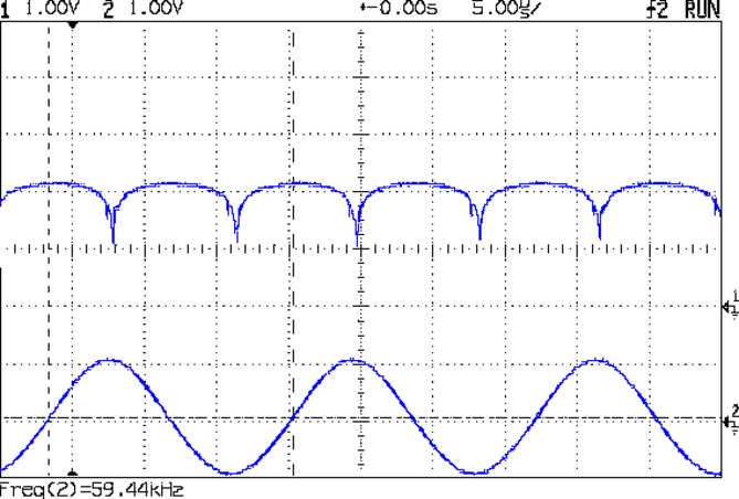
Eyeballometrically, it might be a log response to the absolute value of the derivative: kinda flat on the ups-and-downs, kinda zero-ish at the tops-and-bottoms. Or maybe it’s the log response to a phase-shifted version of the input, with the lows corresponding to the zero crossings.
Documentation for the circuit seems nonexistent, because eBay. Fortunately, one can pop the top to reveal the straightforward PCB layout:
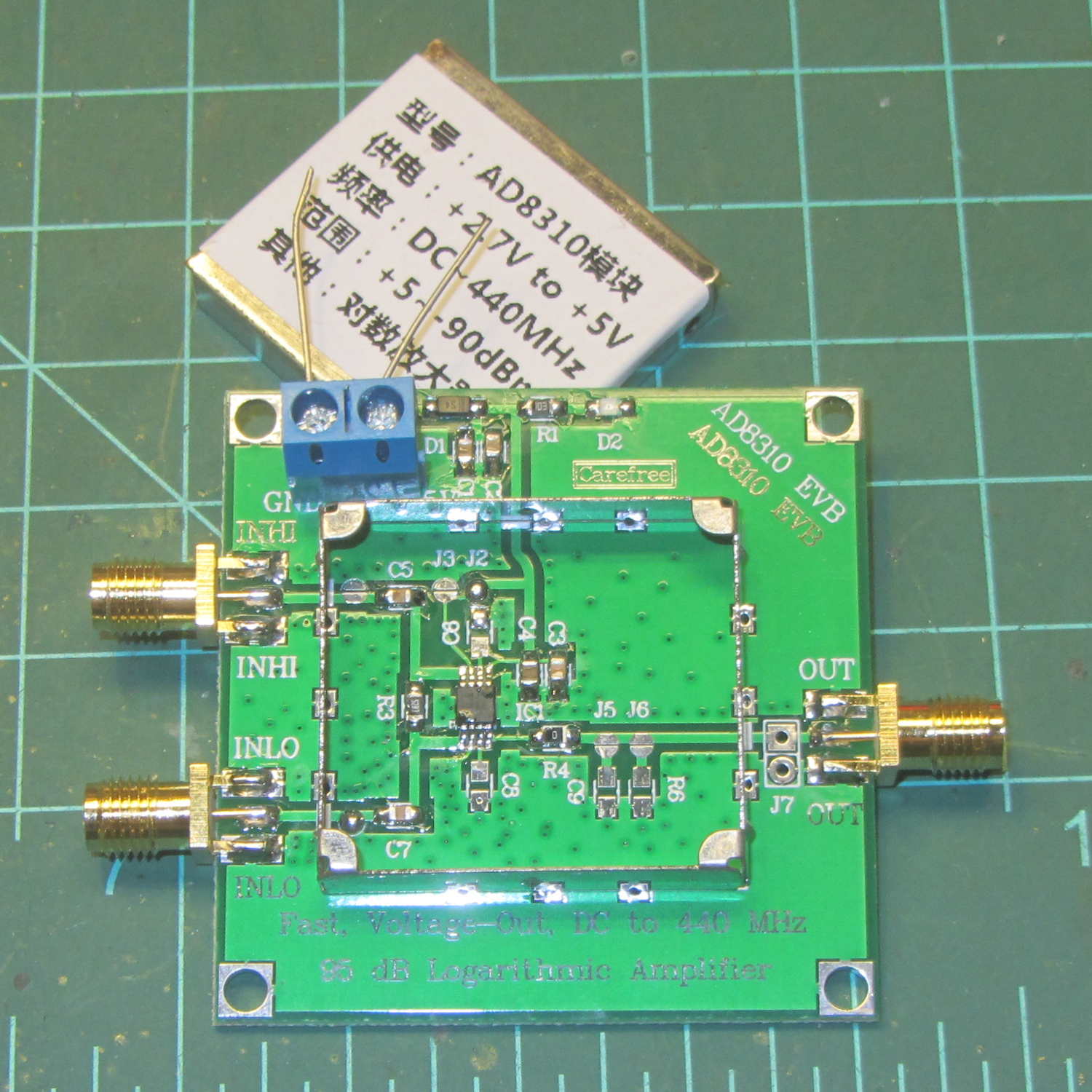
A closer look:

A capacitance meter says input capacitors C5 and C7 are both 10 nF.
A sketch of the circuitry:
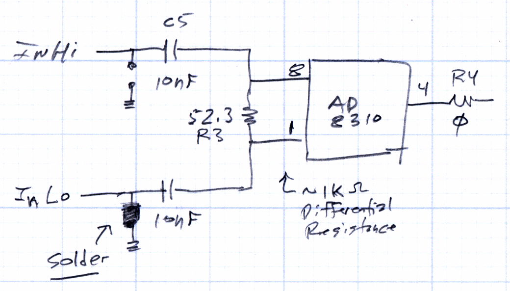
The datasheet puts the terminating resistor on the other side of the input caps, where it surely belongs:

Achtung: the solder blob just to the left of C7 grounds the signal pin on the InLo SMA. Don’t connect anything to InLo which might take offense at having its output shorted to ground; the SMA terminator I used had no effect whatsoever.
The AD8310 chip (assuming that’s what it really is) has a differential input resistance = 1 kΩ and capacitance = 1.4 pF in parallel with R3, the 52.3 Ω terminating resistor, making the net resistance just under 50 Ω.
At 60 kHz, the input caps have a reactance of 270 Ω apiece, which means the “terminating” resistor is maybe 10% of the mostly capacitive input impedance seen at the InHi connector. That means the AD8310 inputs see maybe 10% of the input signal.
In fact, if you regard those three parts as an RC high pass filter and merge the caps into a single 5 nF unit, it rolls off at 620 kHz = 1/(2π · 52 · 5 pF). Obviously, it’ll be a fine differentiator at 1/10 the breakpoint frequency.
A simulation shows it in action (clicky for more dots):
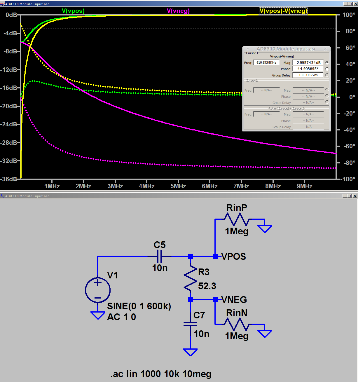
The two 1 MΩ resistors provide a balanced DC path-to-ground for R3 to keep the simulator happy.
The (+) input tends toward 0 dB as C5 tends toward a short, the (-) input tends toward ground as C7 does likewise, but their difference isn’t a constant value. Seeing as how a log amp should respond to small differences, methinks it’s hard at work.
The AD8310 data sheet says the scale factor is about 24 mV/dB between 10 MHz and 200 MHz, with no frequency dependence worth mentioning. Eyeballometrically, the output has a 240 mV = 10 dB straight-line decrease over the entire frequency range of that scope shot. It drops by 220 mV = 9.2 dB in the decade from 50 to 500 MHz, half of the 20 dB you’d expect from a first-order filter response.
The AD8310 has an internal 2 MHz high pass feedback loop to suppress low frequency input offset voltages. The doc recommends a 1 µF cap from OLFT to ground for frequencies down in the low audio range. One might solder the cap across the convenient pads labeled C8 below the chip.
Rearranging the input circuitry seems in order:
- Move R3 outside C5 and C7, per the datasheet
- Increase C5 and C7 to 1 µF -ish
- Add 100nF – 1 µF bypass cap at C8
I have the uneasy feeling I’m overlooking something obvious …
Update – The rest of the story: Corrected Input Circuit and Video Bandwidth Rolloff.

Comments
6 responses to “AD8310 Log Amp Module: LF Response”
I wonder whether placing the termination resistor on the far side of the coupling capacitors was intentional. That would give a nice AC termination but not soak up a DC value, which would be useful in some cases like signals with a DC component or apparatus that’s running both signal and power through a single conductor. However, both populating the InLo SMA connector and grounding out that signal seems odd.
Your uncertainty of whether that’s an actual AD8310 or not is well founded. One of the fields we’re active in is package failure analysis, opening the package to check the wire bonds, or probe the chip itself to find the failure, etc etc. The companies we represent do this with mechanical milling, acid, laser, plasma etch, etc etc. the key is to open the package without damaging the chip. Interestingly, a side market (niche of a niche of a niche) is government agencies wanting to open the packages to test for counterfeits. One of my colleagues told an interesting story where he went to install one of the tools and was given an address that was basically a dirt road off a French autoroute in the midst of nowhere. At the end of the road was a bunker like building with a massive dish behind it. And that’s where they had their little counterfeit busting bureau.
This guy’s schematic is similar to your hand drawn one:
https://www.sv1afn.com/ad8310fastrfd.html
For whatever it’s worth…
– Steve
Spoiler alert: that layout doesn’t work. Putting the terminator directly across the input eliminates the frequency dependence, because the caps act as high-pass filters to the 1.1 kΩ log amp input. The source sees a resistive termination, the amp has DC-isolated inputs, and all is well.
If you’re using the amp with a fixed frequency source that isn’t too fussy about termination and you don’t care about absolute power calibration, then you might be satisfied with the results.
[…] puzzling over the AD8310 Log Amp module’s peculiar frequency response, I hacked up the front end circuitry to match the data sheet’s recommended […]
[…] The part I didn’t understand turned out to be the bandwidth of the final output stage = “video bandwidth”, which defaults to 25 MHz. After fixing the input circuitry, a 25 MHz VBW let the output track a 60 kHz input signal just fine: […]