Ed Nisley's Blog: Shop notes, electronics, firmware, machinery, 3D printing, laser cuttery, and curiosities. Contents: 100% human thinking, 0% AI slop.
Tag: Improvements
Making the world a better place, one piece at a time
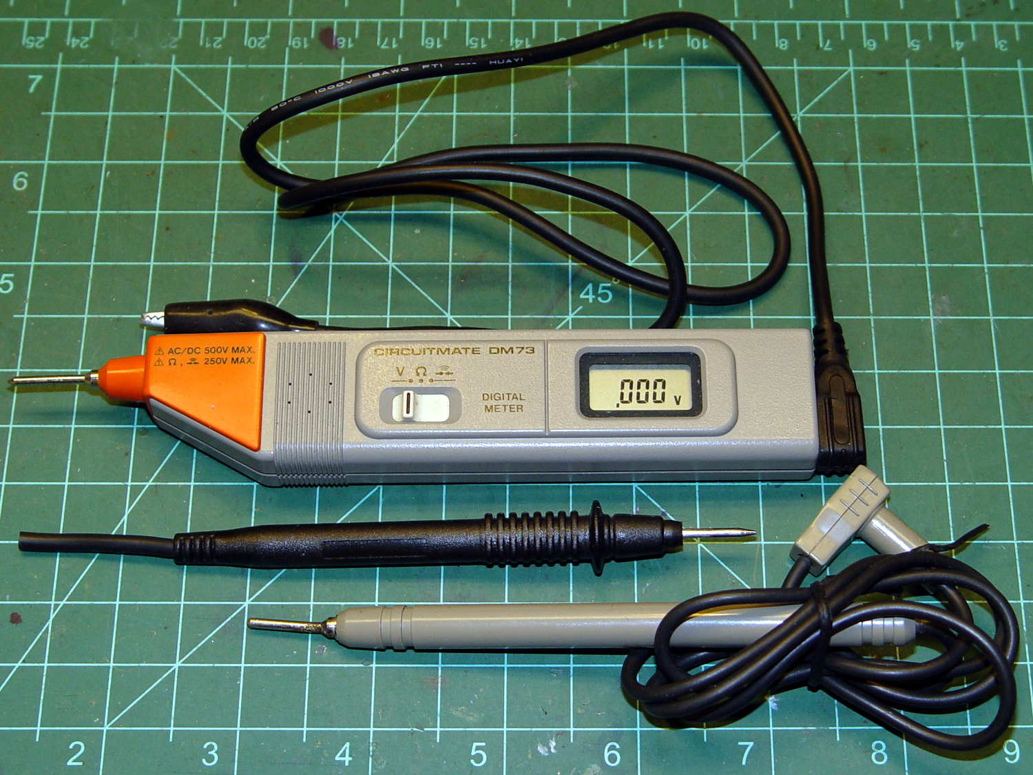
Although it’s rated to 500 V, it violates the fundamental principle of high-voltage electronics debugging:
Always keep one hand in your pocket!
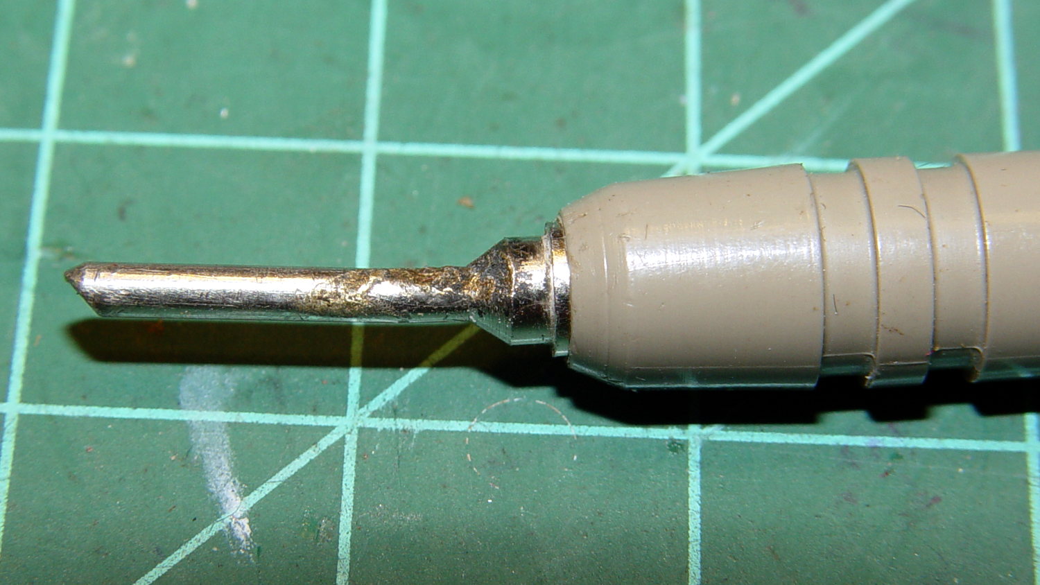
The scorched and truncated probe tip on the “ground wire” shows Phil slipped at least once:
Beckman DM73 – probe tip
After far too long, I sacrificed a black multimeter probe from the heap, soldered an alligator clip on the end, and, henceforth, will use it appropriately. Mostly, I never do any high-voltage work, but you never know.
I suppose I should splice that nice black probe onto the end of the Beckman wire for low-voltage work…
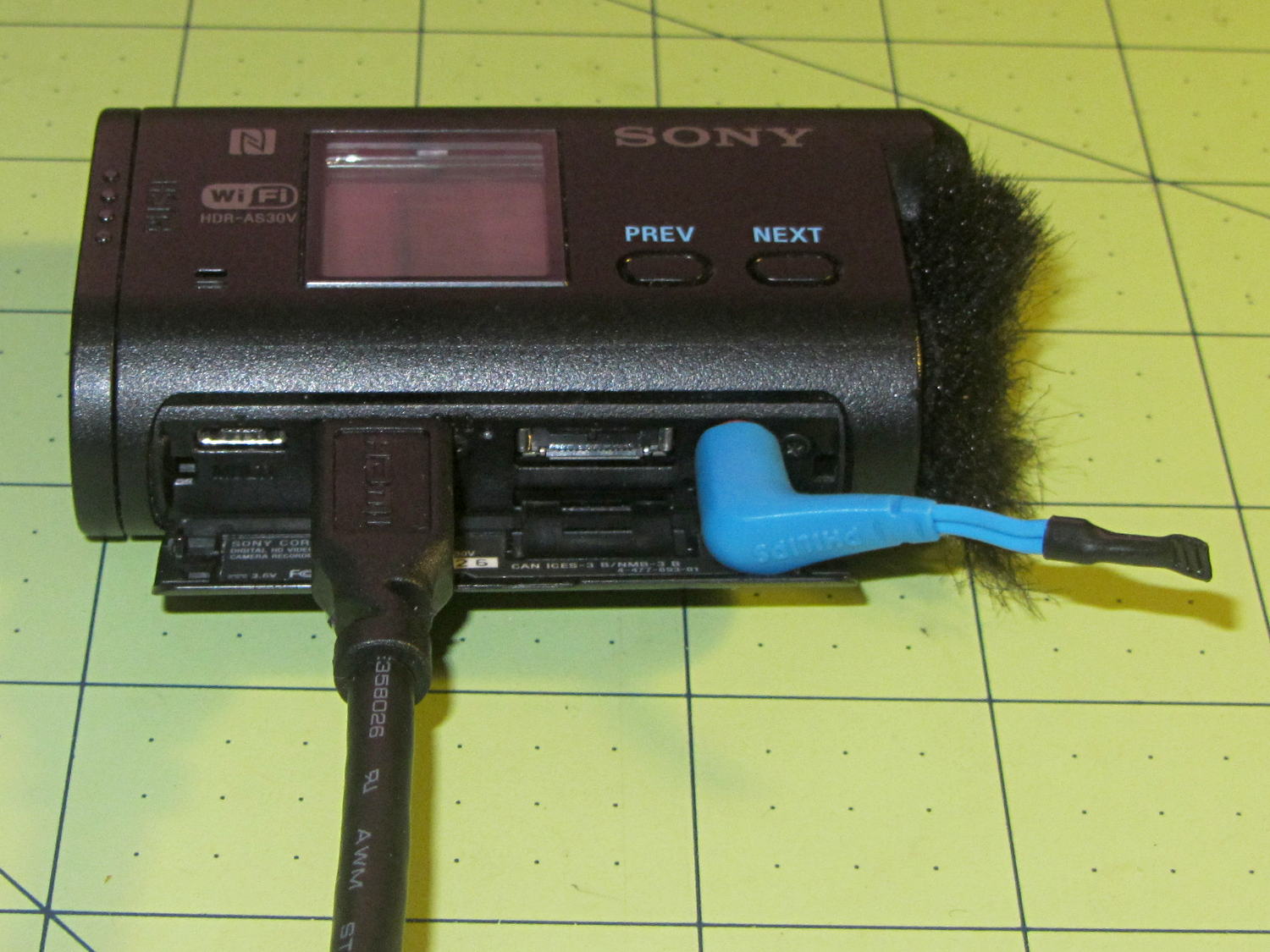
The Sony HDR-AS30V has extremely high audio gain, which is precisely what you need for the mic on an action camera. It sends that audio, along with the video, through its HDMI output, so when you drive a display from the camera in enclosed space, the audio is REALLY LOUD and causes severe feedback. For obscure reasons, given the staggering cost of the venue’s AV system, there’s no way to mute the audio channel of the video input when you’re also using a mic attached to someone giving a presentation.
The obvious solution, a shorted jumper (formerly an earbud plug) in the external mic jack, looked like this:
Sony HDR-AS30V – Dummy external mic
Contrary to what I expected, the camera doesn’t disable the internal mic with the jumper in place. The amp probably uses an analog multiplexer, rather than a mechanical switch, and even an off-channel isolation of, say, 76 dB (from the MAX4544 spec, for example) isn’t enough to completely mute the mic. You could, given sufficient motivation, measure the actual isolation, but the surviving audio isn’t subtle at all.
The not-obvious solution turned out to be putting the camera into either single or interval photo mode, rather than the movie mode I use for bike rides. It seems that when the video format doesn’t require audio, the camera either disables the audio inputs or (more likely) just doesn’t include audio data in the HDMI output.
Which produces exactly what I want: a video output with no accompanying audio.
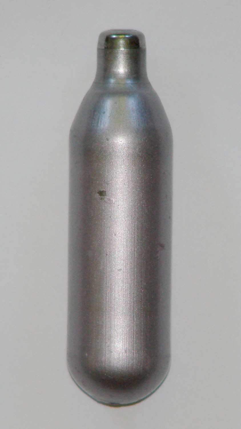
A trio of N2O cartridges / capsules made their way into the Basement Laboratory and cried out to be fitted with fins:
N2O Capsule Fins – installed
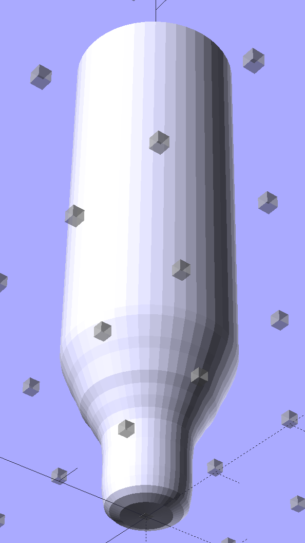
My original model tinkered up a cartridge from solid object primitives, but I’ve since discovered that cheating produces a much better and faster and easier result for cylindrical objects:
N2O Capsule – solid model – bottom view
The trick is getting an image of the original object from the side, taken from far enough away to flatten the perspective:
N2O capsule – side view
Then overlay and scale a grid to match the actual length:
N2O capsule – grid overlay
The grid has 1 mm per minor square, centered along the cartridge’s axis, and zeroed at the tip; I rotated the cartridge image by half a degree to line it up with the grid.
Print it out on actual paper so you can eyeball the measurements and write ’em where you need ’em:
N2O capsule – grid overlay – printed
Which becomes an OpenSCAD polygon definition:
RADIUS = 0;				// subscript for radius values
HEIGHT = 1;				//   ... height above Z=0 at seal flange

//-- N2O 8 g capsule

CartridgeOutline = [			// X values = measured radius, Y as distance from tip
	[0.0,0.0],					//  0 cartridge seal tip
	[2.5,0.1],					//  1 seal disk
	[3.5,0.5],[4.0,1.0],		//  2 tip end
	[4.2,2.0],[4.3,3.0],		//  4 tip
	[4.3,6.0],					//  6 chamfer
	[4.5,8.0],					//  7 taper
	[4.9,9.0],					//  8
	[5.5,10.0],					//  9
	[6.0,11.0],					// 10
	[6.7,12.0],					// 11
	[7.1,13.0],					// 12
	[7.5,14.0],					// 13
	[8.0,15.0],					// 14
	[8.4,16.0],					// 15
	[8.8,17.0],					// 16
	[9.0,18.0],[9.0,58.0],		// 17 body
	[0.0,65.0]					// 19 dummy end cone
	];

TipLength = CartridgeOutline[6][HEIGHT];
TipOD = 2*CartridgeOutline[5][RADIUS];

BodyOD = 2*CartridgeOutline[17][RADIUS];
BodyOAL = CartridgeOutline[19][HEIGHT];
Because the rounded end of the cartridge doesn’t matter, I turned it into a cone.
Which then punches a matching dent in the fin structure:
Gas Capsule Fins – Slic3r preview
The lead picture doesn’t quite match the Slic3r preview, as I found the single-width diagonal fins weren’t strong enough. Making them two (nominal) threads wide lets Slic3r lay down three thinner threads in the same space:
Gas Capsule Fins – thicker – Slic3r preview
That’s letting Slic3r automagically determine the infill and perimeter thread width to make the answer come out right. As nearly as I can tell, the slicing algorithms have become smart enough to get the right answer nearly all of the time, so I can-and-should relinquish more control over the details.
The OpenSCAD source code:
// CO2 capsule tail fins
// Ed Nisley KE4ZNU - October 2015
Layout = "Build"; // Show Build FinBlock Cartridge Fit
//-------
//- Extrusion parameters must match reality!
// Print with +0 shells and 3 solid layers
ThreadThick = 0.25;
ThreadWidth = 0.40;
HoleWindage = 0.2;
Protrusion = 0.1; // make holes end cleanly
function IntegerMultiple(Size,Unit) = Unit * ceil(Size / Unit);
//-------
// Capsule dimensions
CartridgeSides = 12*4; // number of sides
RADIUS = 0; // subscript for radius values
HEIGHT = 1; // ... height above Z=0 at seal flange
//-- N2O 8 g capsule
RW = HoleWindage/2; // enlarge radius by just enough
CartridgeOutline = [ // X values = measured radius, Y as distance from tip
[0.0,0.0], // 0 cartridge seal tip
[2.5 + RW,0.1], // 1 seal disk
[3.5 + RW,0.5],[4.0 + RW,1.0], // 2 tip end
[4.2 + RW,2.0],[4.3 + RW,3.0], // 4 tip
[4.3 + RW,6.0], // 6 chamfer
[4.5 + RW,8.0], // 7 taper
[4.9 + RW,9.0], // 8
[5.5 + RW,10.0], // 9
[6.0 + RW,11.0], // 10
[6.7 + RW,12.0], // 11
[7.1 + RW,13.0], // 12
[7.5 + RW,14.0], // 13
[8.0 + RW,15.0], // 14
[8.4 + RW,16.0], // 15
[8.8 + RW,17.0], // 16
[9.0 + RW,18.0],[9.0 + RW,58.0], // 17 body
[0.0,65.0] // 19 dummy end cone
];
TipLength = CartridgeOutline[6][HEIGHT];
TipOD = 2*CartridgeOutline[5][RADIUS];
CylinderBase = CartridgeOutline[17][HEIGHT];
BodyOD = 2*CartridgeOutline[17][RADIUS];
BodyOAL = CartridgeOutline[19][HEIGHT];
//-------
// Fin dimensions
FinThick = 1.5*ThreadWidth; // outer square
StrutThick = 2.0*ThreadWidth; // diagonal struts
FinSquare = 1.25*BodyOD;
FinTaperLength = sqrt(2)*FinSquare/2 - sqrt(2)*FinThick - ThreadWidth;
FinBaseLength = 0.7 * CylinderBase;
FinTop = 0.9*CylinderBase;
//-------
module PolyCyl(Dia,Height,ForceSides=0) { // based on nophead's polyholes
Sides = (ForceSides != 0) ? ForceSides : (ceil(Dia) + 2);
FixDia = Dia / cos(180/Sides);
cylinder(r=(FixDia + HoleWindage)/2,h=Height,$fn=Sides);
}
module ShowPegGrid(Space = 10.0,Size = 1.0) {
Range = floor(50 / Space);
for (x=[-Range:Range])
for (y=[-Range:Range])
translate([x*Space,y*Space,Size/2])
%cube(Size,center=true);
}
//-------
// CO2 cartridge outline
module Cartridge() {

 rotate_extrude($fn=CartridgeSides)
 polygon(points=CartridgeOutline);

}
//-------
// Diagonal fin strut
module FinStrut() {
intersection() {
rotate([90,0,45])
translate([0,0,-StrutThick/2])
linear_extrude(height=StrutThick)
polygon(points=[
[0,0],
[FinTaperLength,0],
[FinTaperLength,FinBaseLength],
[0,(FinBaseLength + FinTaperLength)]
]);
translate([0,0,FinTop/2])
cube([2*FinSquare,2*FinSquare,FinTop], center=true);
}
}
//-------
// Fin outline
module FinBlock() {
$fn=12;
render(convexity = 4)
union() {
translate([0,0,FinBaseLength/2])
difference() {
intersection() {
minkowski() {
cube([FinSquare - 2*ThreadWidth,
FinSquare - 2*ThreadWidth,
FinBaseLength],center=true);
cylinder(r=FinThick,h=Protrusion,$fn=8);
}
cube([2*FinSquare,2*FinSquare,FinBaseLength],center=true);
}
difference() {
cube([(FinSquare - 2*FinThick),
(FinSquare - 2*FinThick),
(FinBaseLength + 2*Protrusion)],center=true);
for (Index = [0:3])
rotate(Index*90)
translate([(FinSquare/2 - FinThick),(FinSquare/2 - FinThick),0])
cylinder(r=2*StrutThick,h=(FinBaseLength + 2*Protrusion),center=true,$fn=16);
}
}
for (Index = [0:3])
rotate(Index*90)
FinStrut();
rotate(180/12)
cylinder(d=IntegerMultiple(TipOD + 6*ThreadWidth,ThreadWidth),h=TipLength);
}
}
//-------
// Fins
module FinAssembly() {
difference() {
FinBlock();
translate([0,0,2*ThreadThick]) // add two layers to close base cylinder
Cartridge();
}
}
module FinFit() {
translate([0,0.75*BodyBaseLength,2*ThreadThick])
rotate([90,0,0])
difference() {
translate([-FinSquare/2,-2*ThreadThick,0])
cube([IntegerMultiple(FinSquare,ThreadWidth),
4*ThreadThick,
1.5*BodyBaseLength]);
translate([0,0,5*ThreadWidth])
Cartridge();
}
}
//-------
// Build it!
ShowPegGrid();
if (Layout == "FinStrut")
FinStrut();
if (Layout == "FinBlock")
FinBlock();
if (Layout == "Cartridge")
Cartridge();
if (Layout == "Show") {
FinAssembly();
color("LightYellow") Cartridge();
}
if (Layout == "Fit")
FinFit();
if (Layout == "Build")
FinAssembly();
The big bag o’ new-old-stock Inmac ball-point plotter pens had five different colors, so I popped a black ceramic tip pen in Slot 0 and ran off Yet Another Superformula Demo Plot:
HP 7475A – Inmac ball pens – weak blue
All the ball pens produce spidery lines, but the blue pen seemed intermittent. Another blue pen from the bag behaved the same way, so I pulled the tip outward and tucked a wrap of fine copper wire underneath. You can see the wire peeking out at about 5 o’clock, with the end at 3-ish:
HP 7475A – Inmac ball pen – wire spacer
The wire holds the tip slightly further away from the locating flange and, presumably, makes it press slightly harder against the paper:
HP 7475A – Inmac ball pen – stock vs. extended
A bit more pressure helped, but not enough to make it dependable, particularly during startup on the legend characters:
HP 7475A – Inmac ball pens – extended blue
That black line comes from an ordinary fiber-tip pen that looks like a crayon on a paper towel by comparison with the hair-fine ball point lines.
Delicacy doesn’t count for much in these plots, so I’ll save the ball pens for special occasions. If, that is, I can think of any…
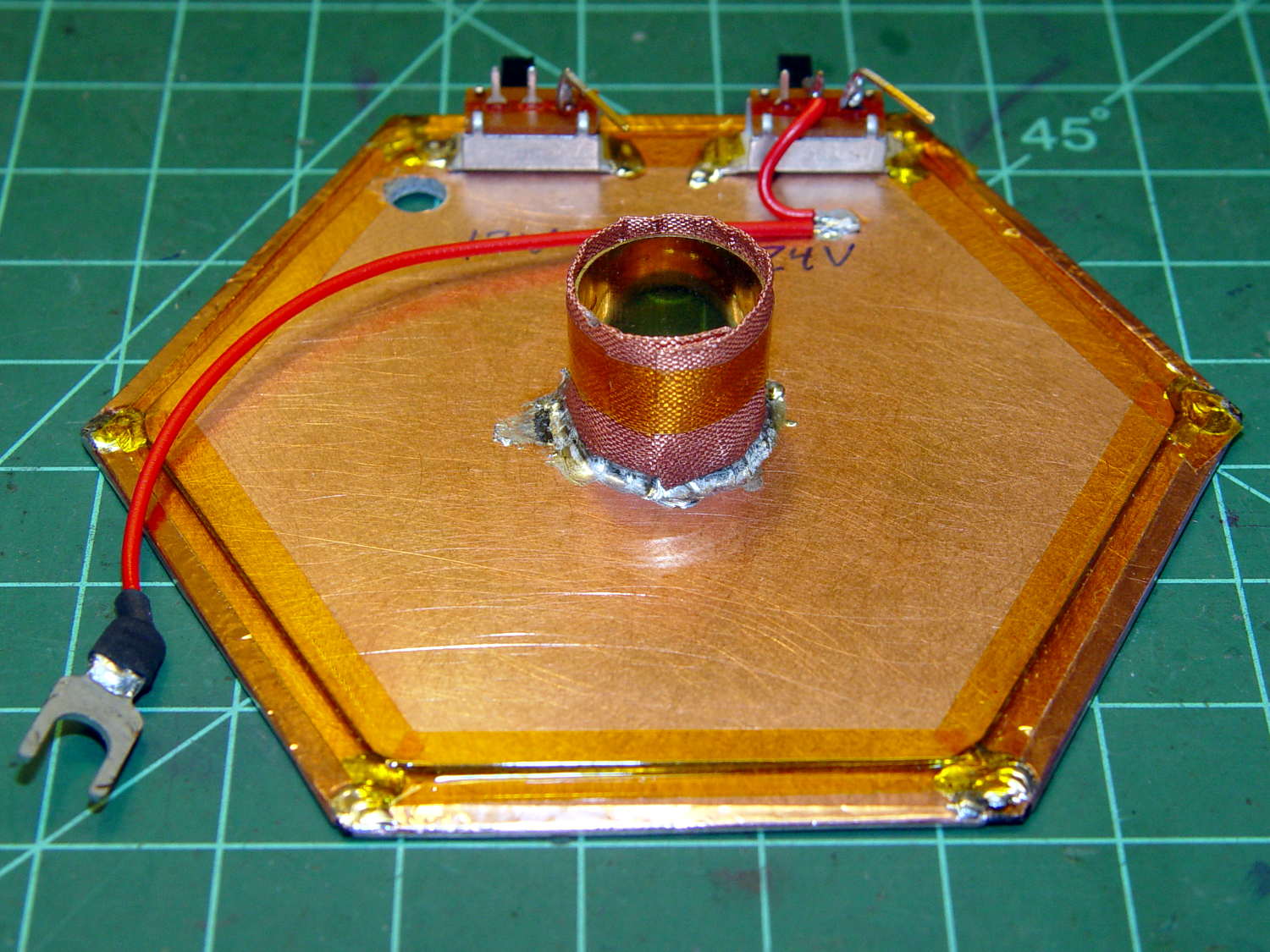
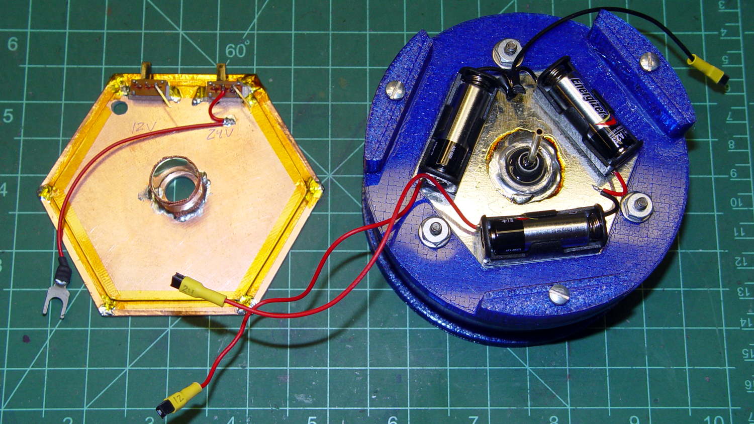
An undrilled double-sided circuit board with the edges bonded together doesn’t look like much:
Electrometer amp – undrilled shield planes
Soldering a smaller hex to the center of the bonded plate produces an isolated plane:
Electrometer amp – finished shield planes
The copper fabric tape wrapped around a brass tube soldered to the isolated plane contacts the ionization chamber shell around the central contact and (should) provide complete shielding. Kapton tape around the edges reduces the likelihood of inadvertent shorts.
Working with a shield at +24 V gave me the shakes, so this one confines the chamber bias to the isolated hex and shell, with the larger hex at circuit common (a.k.a. ground). The isolated plane has about 275 pF to the ground plane, which isn’t a Bad Thing at all. In principle, the chamber bias doesn’t need a switch, because there’s no current drain, but I vastly prefer having cold circuitry before popping the lid.
If I had a small DPST switch, I’d use it:
Electrometer amp – chamber – shield planes
As it stands, one switch controls the +24 V chamber bias and the other switches +12 V power to the electrometer amp front end, with simpleminded connectors so I can separate the pieces.
We’ll see how well all that works in practice.
An alert reader will notice the tiny difference between the blue PETG shapes in the two pictures. The bottom one comes from the revised code, of course.
It has a number of shortcomings (notice the padding taped to the corner of the useless drawers), but the most pressing problem was that it didn’t quite line up with the table top in the Basement Sewing Room. After some pondering, we decided to shorten the legs and install leveling screws.
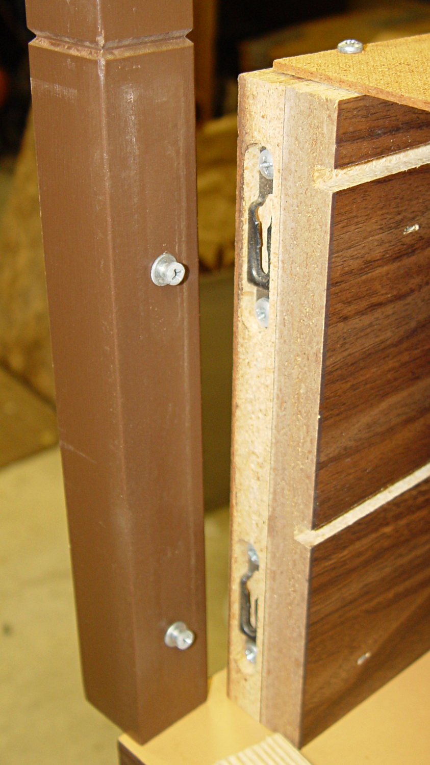
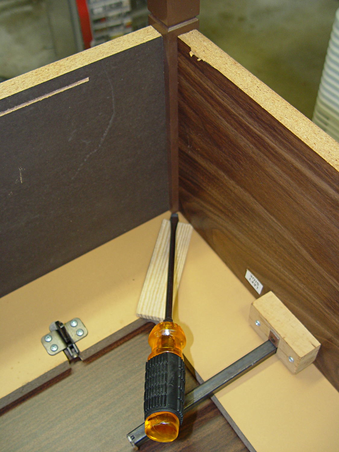
The first problem was figuring out how to dismantle the thing. It turns out the legs have completely hidden joint hardware:
Sears Sewing Table – leg joint hardware
They’re obviously intended as assemble-only fittings, but prying from the inside of the corners will put the tool marks where they can’t be seen:
Sears Sewing Table – leg removal
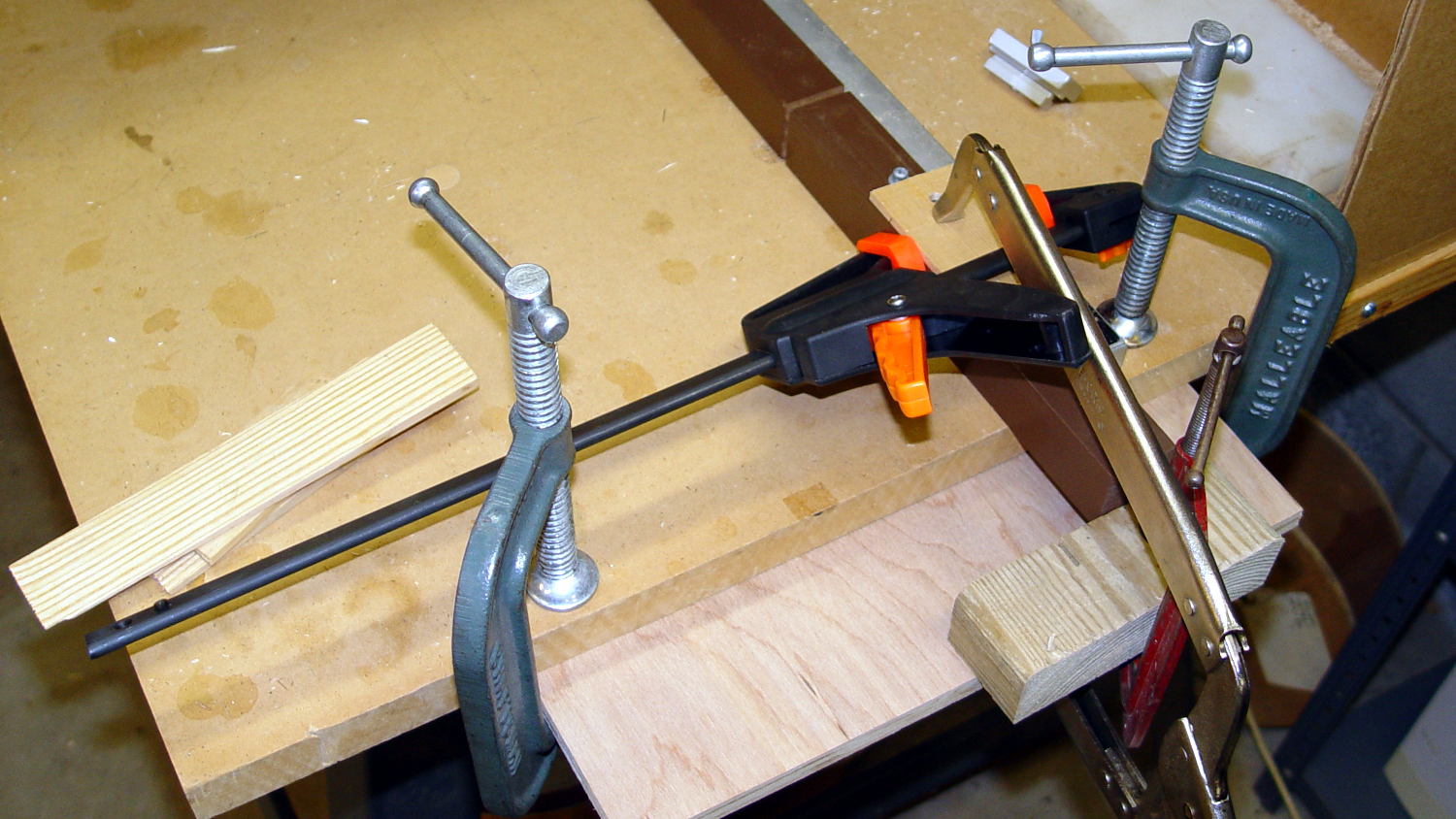
The legs taper below the fittings and require shims to prevent horrible saw accidents:
Sears Sewing Table – leg shortening
Another in my continuing series of Why You Can Never Have Too Many Clamps shows the square section of the leg aligned with the saw fence:
Sears Sewing Table – leg clamps
And when the cuttin’ were done, it turned out that the table had two different types of legs with (at least) two different lengths:
Sears Sewing Table – leg cutoffs
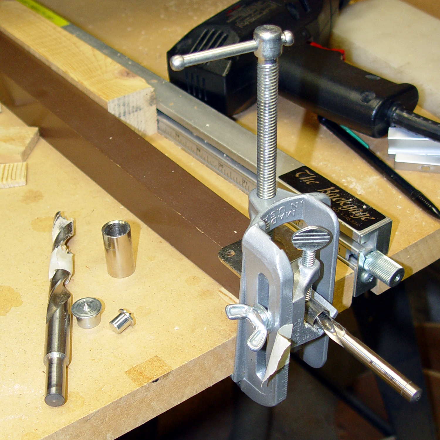
I have a bunch of 5/16 inch feet from some random industrial hardware, so I drilled a 5/16 inch hole into the legs, using a doweling jig and more shims:
Sears Sewing Table – leg drilling setup – overview
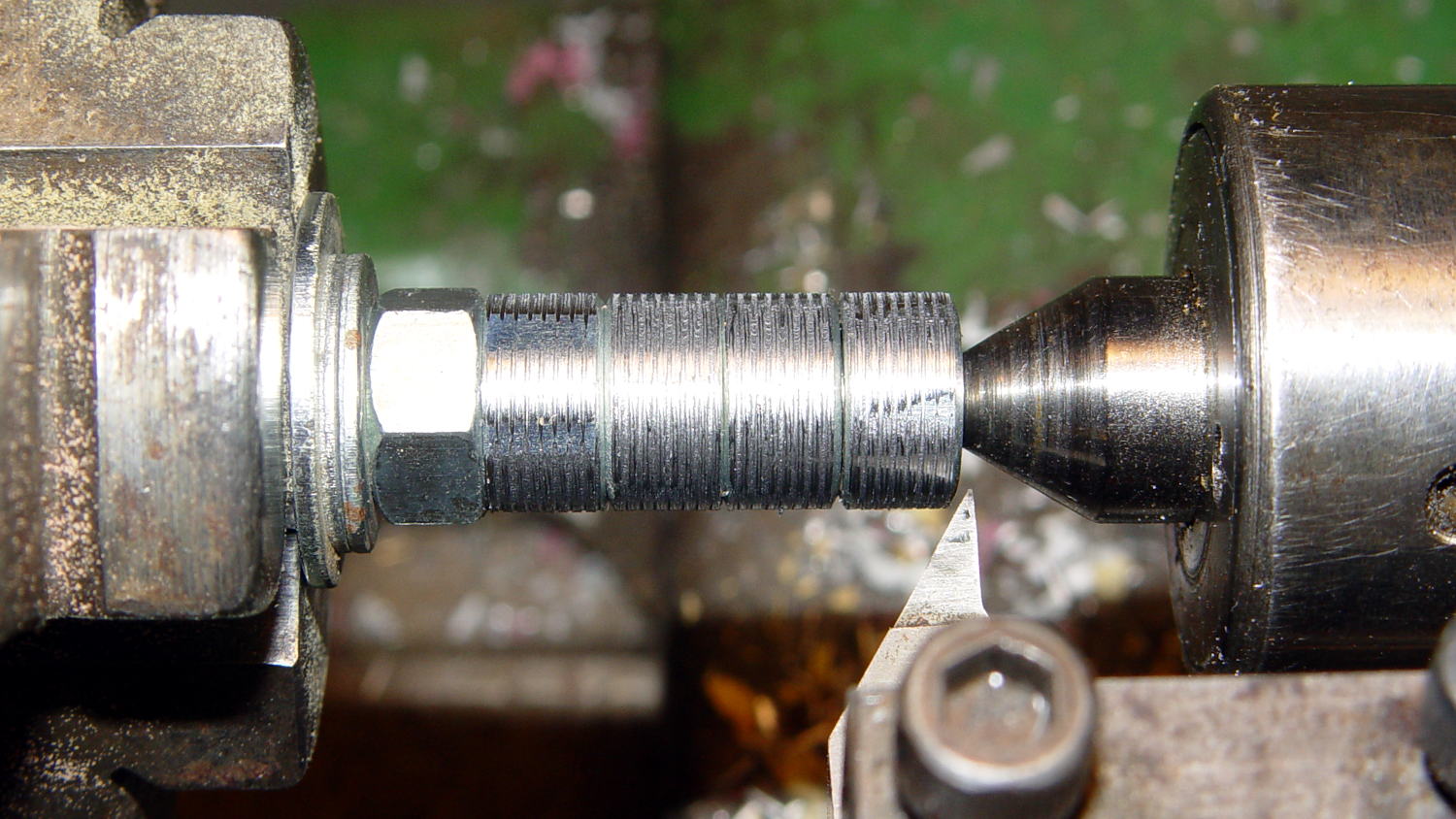
Normally, you’d bang a T-nut into each leg, but I thought those spikes would split the minimal wood remaining around the hole, so I turned the corners off a quartet of ordinary hex nuts and laid a coarse groove along their length:
Sears Sewing Table – preparing nut inserts
The modified nuts are 1/2 inch OD and you should drill that hole before the longer 5/16 inch clearance hole. I’ll eventually dab some epoxy in the holes, seat the nuts, and that’ll be a permanent installation with no risk of cracking the legs.
The snippet of tape on the doweling jig remembers the drill guide position, but the legs were sufficiently different that each one required different shims and some hand-tuning:
Sears Sewing Table – leg drilling setup – detail
I dry-assembled the table in anticipation of more modifications. Basically, you wiggle-jiggle the leg studs into their latches, then whack the end of the leg with a rubber mallet to seat it against the underside of the tabletop.
Slicing another half inch off the legs seems like a Good Idea that should better match the upstairs table. Mary also wants to round off the drawers and remove a bit of the front panel, which will require dismantling the entire table, but that can wait for a pause in the quilting.