Ed Nisley's Blog: Shop notes, electronics, firmware, machinery, 3D printing, laser cuttery, and curiosities. Contents: 100% human thinking, 0% AI slop.
Category: Science
If you measure something often enough, it becomes science
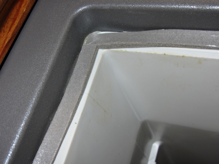
A bit of rummaging in the Big Box o’ Weatherstripping produced the stub end of a spool bearing 1/4 x 1/8 foam tape that exactly fills the gap between the Basement Safe’s door and liner:
Basement Safe – Foam door seal – latch side
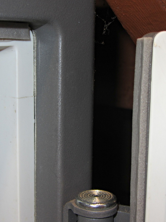
The hinge side of the door has tape between the door liner and the safe wall, because that closes in compression rather than shear:
Basement Safe – Foam door seal – hinge side
There should be a big bump in the humidity record marking that installation, but I don’t expect any immediate difference. If the silica gel lasts more than two months, I’ll consider it a win.
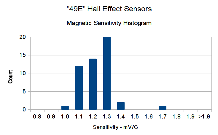
A bag of 50 cheap Hall effect sensors arrived from the usual eBay vendor, who was different from all previous eBay vendors (if in name only). Passing 124 mA through the armored FT50 toroid with 25 turns of 26 AWG wire, we find this distribution of bias points, measured as the offset from the actual VCC/2:
eBay 49E Hall Effect Sensor Bias Histogram
The bias point is actually referenced to the negative terminal (usually ground) with a ±0.25 V variation around the nominal. SS49 sensors run about 0.5 V below VCC/2 (2.25 V with a 5 V supply), SS49E sensors at 2.5 V with a tighter VCC limit that suggests you better stay pretty close to 5.0 V.
Allowing for the fact that I really don’t have good control over the actual magnetic field, the gain distribution seems tight:
eBay 49E Hall Effect Sensor Sensitivity Histogram
You’ll recall the Genuine Honeywell sensor specs:
SS49 – nominal 0.9 mV/G, limits 0.6 to 1.25 mV/G
SS49E – nominal 1.4 mV/G, limits 1.0 to 1.75 mV/G
The gain is roughly half that of the previous “49E” sensors, confirmed by sticking one of them this field. I don’t know which is more accurate, but these have a much prettier distribution.
So this lot resembles 49E sensors in both bias and gain.
Given the bias variation, though, it’s obvious that a DC application must measure the zero-field output and apply an analog offset to the amplifier, because a twiddlepot setting won’t suffice. Most likely, you’d want to update the offset every now and again to compensate for temperature variation, too.
Tossing the outliers gives an average gain of 1.17, which would give results within 10% over the lot. Given that you don’t care about the actual magnetic field, you could calibrate the output voltage for a known input current and get really nice results.
If you were doing position sensing from a known magnet, you’d want better control of the magnetic field gradient.
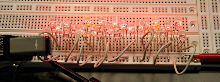
The collection of LEDs that I’ve been abusing with 100 mA pulses at 20% duty cycle got lined up in parallel, with three LEDs in series, driven from a bench power supply set to limit the current to about 180 mA:
Series-parallel LED test fixture
I sweetened the mix by adding a few other LEDs that had served their time in hell, then took some data by clipping the Tek Hall effect current probe around each of the white wires in turn:
Color
LED1
LED2
LED3
Divisions
Current – mA
Total voltage
Red
1.98
1.98
1.94
4.7
23.5
5.90
Red
1.95
1.95
2.00
3.4
17.0
5.90
Red
1.97
1.97
1.97
5.1
25.5
5.91
Yellow
1.97
1.97
1.96
4.5
22.5
5.90
Yellow
1.97
1.96
1.97
4.6
23.0
5.90
Red
1.98
1.98
1.94
4.6
23.0
5.90
Red
1.95
1.95
2.00
3.3
16.5
5.90
Red (new!)
1.99
1.96
1.94
6.4
32.0
5.89
Despite the decimals, don’t trust anything beyond the first two digits.
The LEDs started out with 6.03 V across them at that current, then settled down to 5.92 V after a few minutes of warming up.
The “new” Red string replaces a trio of old LEDs incinerated by a DVM probe fumble. They have a much higher current at the same voltage; the older LEDs have been abused enough to pass a lower current.
As an experiment, I swapped the LED with the 2.00 V drop in the string with the lowest current (line 7) and the LED with the 1.94 V drop in a string with higher current (line 6), only to find that the current followed the LEDs. Evidently, those LEDs were the limiting factor, even though their forward drops weren’t the same in their new strings.
So it seems binning based on forward drop doesn’t help much. Perhaps just line up a bunch of three-LED strings (forcing all of them to see the same forward drop), measure their current, and reject the highest and lowest strings to get a decent match among the remainder?
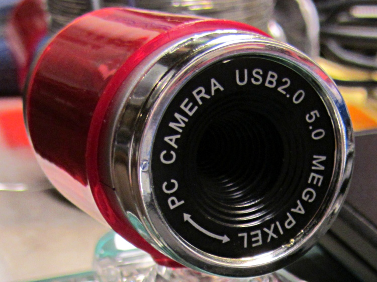
A brace of “Fashion” USB video cameras arrived from halfway around the planet. According to the eBay description and the legend around the lens, they’re “5.0 Megapixel”:
Fashion USB camera – case front
The reality, of course, is that for five bucks delivered you get 640×480 VGA resolution at the hardware level and their Windows driver interpolates the other 4.7 megapixels. VGA resolution will be good enough for my simple needs, particularly because the lens has a mechanical focus adjustment; the double-headed arrow symbolizes the focus action.
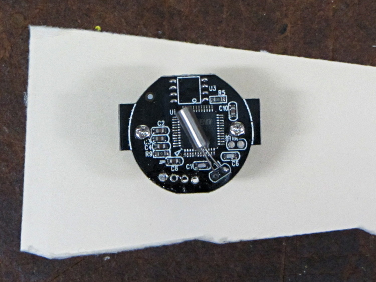
But the case seemed entirely too bulky and awkward. A few minutes with a #0 Philips screwdriver extracted the actual camera hardware, which turns out to be a double-sided PCB with a lens assembly on the front:
Fashion USB video – case vs camera
The PCB has asymmetric tabs that ensure correct orientation in the case:
Fashion USB camera – wired PCB rear
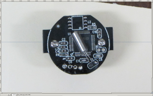
In order to build an OpenSCAD model for a more compact case, we need the dimensions of that PCB and those tabs…
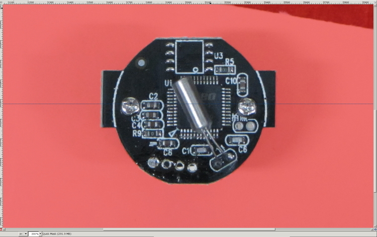
Start with a picture of the back of the PCB against white paper, taken from a few feet to flatten the perspective:
img_3300 – Camera PCB on white paper
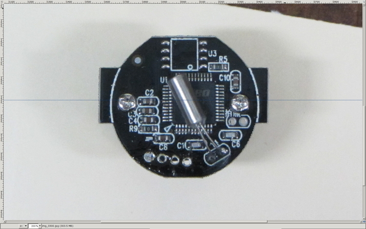
Load it into The GIMP, zoom in, and pull a horizontal guide line down to about the middle of the image:
Camera PCB – horizontal guide – scaled
Rotate to align the two screws horizontally (they need not be centered on the guide, just lined up horizontally):
Camera PCB – rotated to match horizontal guide – scaled
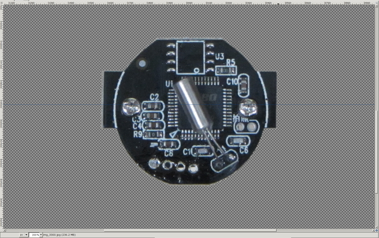
Use the Magic Scissors to select the PCB border (it’s the nearly invisible ragged dotted outline):
Camera PCB – scissors selection – scaled
Flip to Quick Mask mode and clean up the selection as needed:
Camera PCB – quick mask cleanup – scaled
Flip back to normal view, invert the selection (to select the background, not the PCB), and delete the background to isolate the PCB:
Camera PCB – isolated – scaled
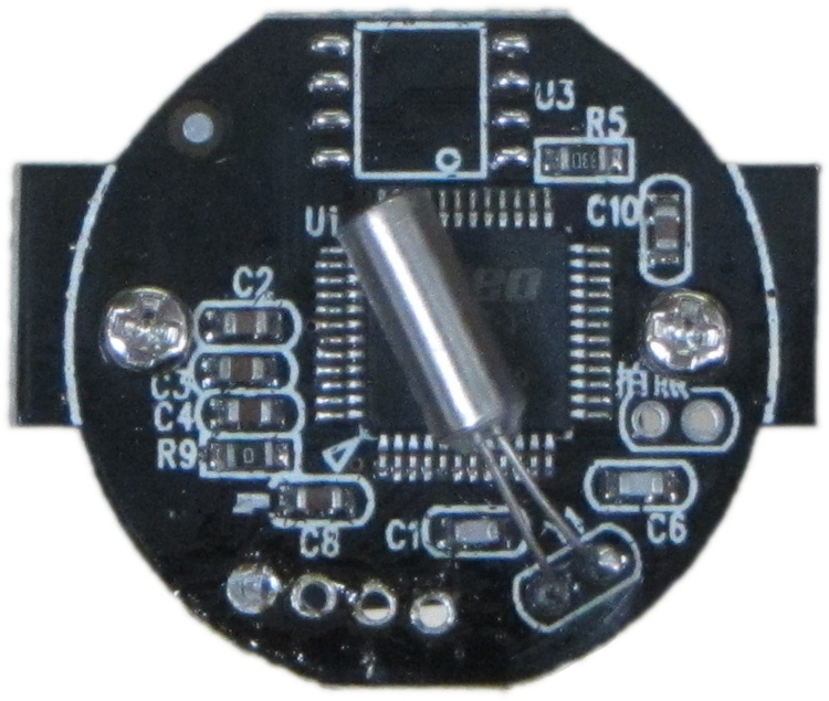
Tight-crop the PCB and flatten the image to get a white background:
Camera PCB – isolated – scaled
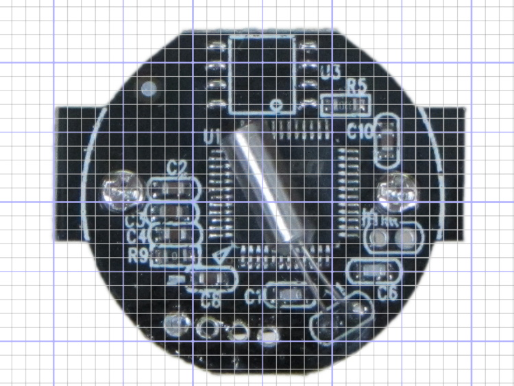
Fetch some digital graph paper from your favorite online source. The Multi-color (Light Blue / Light Blue / Light Grey) Multi-weight (1.0×0.6×0.3 pt) grid (1 / 2 / 10) works best for me, but do what you like. Get a full Letter / A4 size sheet, because it’ll come in handy for other projects.
Open it up (converting at 300 dpi), turn it into a layer atop the PCB image, use the color-select tool to select the white background between the grid lines, then delete the selection to leave just the grid with transparency:
Camera PCB with grid overlay – unscaled
We want one minor grid square to be 1×1 mm on the PCB image, sooo…
Accurately measure a large feature on the real physical object: 27.2 mm across the tabs
Drag the grid to align a major line with one edge of the PCB
Count the number of minor square across to the other side of the image: 29.5
Scale the grid overlay layer by image/physical size: 1.085 = 29.5/27.2
Drag the grid so it’s neatly centered on the object (or has a major grid intersection somewhere useful)
That produces a calibrated overlay:
Camera PCB with grid overlay
Then it’s just a matter of reading off the coordinates, with each minor grid square representing 1.0 mm in the real world, and writing some OpenSCAD code…
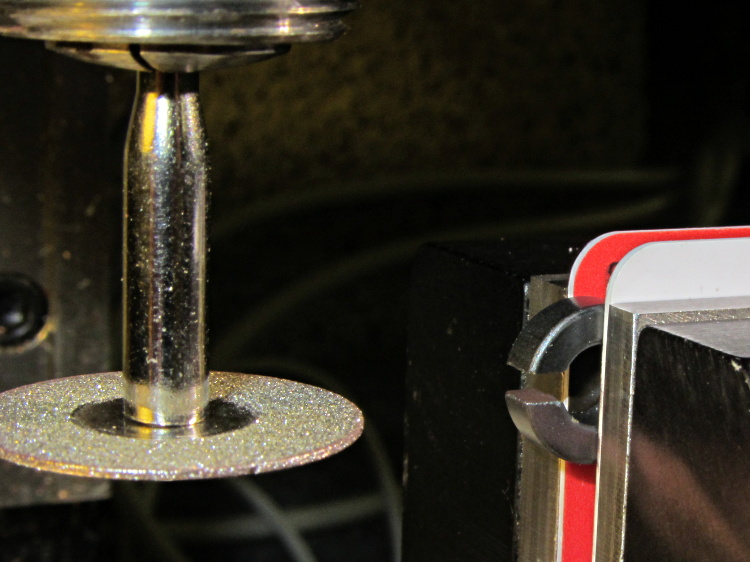
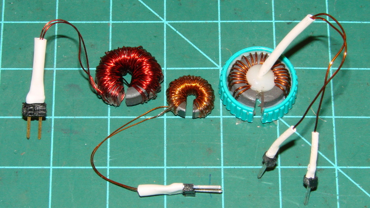
Then wound them with grossly excessive amounts of wire (the up-armored core on the right appeared earlier):
Slit Ferrite Toroid current sensors
The smaller toroid is an FT37-43 that barely covers the active area of an SS49-style Hall effect sensor, but experience with the FT50 toroid suggests that’ll be entirely enough:
slit FT37 toroid trial fit to SS48-style Hall effect sensor
Data on the uncut toroids:
Property
FT50-61
FT37-43
Outer diameter (OD) – inch
0.50
0.375
Inner diameter (ID) – inch
0.281
0.187
Length – inch
0.188
0.125
Cross section area – cm2
0.133
0.133
Mean path length (MPL) – cm
3.02
2.15
Volume – cm3
0.401
0.163
Relative Permeability (μr )
125
850
Saturation flux G @ 10 Oe
2350
2750
Inductance factor (AL) – nH/turn2
68.0
420
Those overstuffed windings improved the sensitivity, but increased the winding resistance far beyond what’s reasonable.
Data on the slit toroids:
Toroid ID
FT50-61
FT37-43
FT50-61
Measured air gap – cm
0.15
0.15
0.17
Winding data
Turns
120
80
25
Wire gauge – AWG
28
32
26
Winding resistance – mΩ
530
920
100
Predicted B field – G/A
872
660
163
Hall effect sensor @ 1.9 mV/G
Predicted output – mV/mA
1.7
1.3
0.31
Actual output – mV/mA
1.9
1.9
0.37
Actual/predicted ratio – %
+12
+46
+19
The last few lines in that table show the transimpedance (transresistance, really, but …) based on the winding current to Hall sensor output voltage ratio (in either mV/mA or V/A, both dimensionally equivalent to ohms), which is why the toroid’s internal magnetic flux doesn’t matter as long as it’s well below saturation.
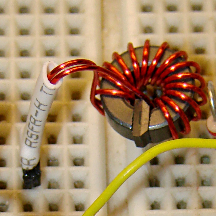
Gnawing the 80 turn winding off the FT37-43 toroid and rewinding it with 15 turns of 24 AWG wire dropped the winding resistance to 23 mΩ and the transimpedance to 0.36 mV/mA:
FT37-43 with 15 turns 24 AWG – Hall sensor
However, applying a voltage gain of about 28 (after removing the sensor’s VCC/2 bias) will produce a 0-to-5 V output from 500 mA input, which seems reasonable.
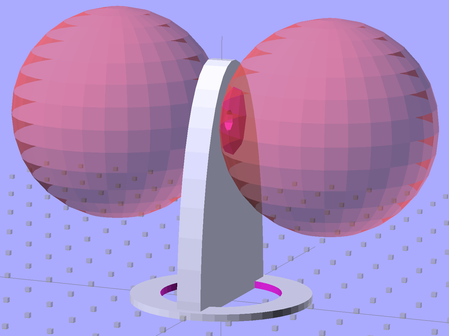
Then generate the sphere (well, two spheres, one for each dent) and offset it to scoop out the dent:
for (i=[-1,1]) {
	translate([i*(DentSphereRadius + HandleThick/2 - DentDepth),0,StringHeight])
		sphere(r=DentSphereRadius);
HandleThick controls exactly what you’d expect. StringHeight sets the location of the hole punched through the handle for a string, which is also the center of the dents.
The spheres have many facets, but only a few show up in the dent. I like the way the model looks, even if the facets don’t come through clearly in the plastic:
Quilting circle template – handle dent closeup – solid model
It Just Works and the exact math produces a better result than by-guess-and-by-gosh positioning.
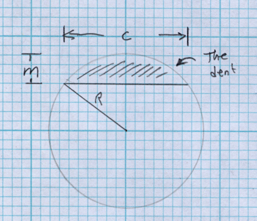
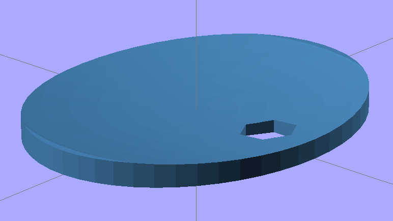
The sphere radius will come out crazy large for very shallow dents. Here’s the helmet plate for my Bicycle Helmet Mirror Mount, which has an indentation (roughly) matching the curve on the side of my bike helmet:
Helmet mirror mount – plate
Here’s the sphere that makes the dent, at a somewhat different zoom scale:
Helmet mirror mount – plate with sphere
Don’t worry: trust the math, because It Just Works.
You find equations like that in Thomas Glover’s invaluable Pocket Ref. If you don’t have a copy, fix that problem right now; I don’t get a cut from the purchase, but you’ll decide you owe me anyway. Small, unmarked bills. Lots and lots of small unmarked bills…