Ed Nisley's Blog: Shop notes, electronics, firmware, machinery, 3D printing, laser cuttery, and curiosities. Contents: 100% human thinking, 0% AI slop.
A semitrailer load of scrap metal pulled into an I-90 rest stop just after we arrived:
Metal scrap trailer – Cutting edge
Apparently, they dump the scrap into the trailer from a great height and, sometimes, a bar can gash the aluminum side wall. That slice obviously predates the current load, but you can see how it happened: dump a load atop a bar leaning against the side and you get a giant metal shear.
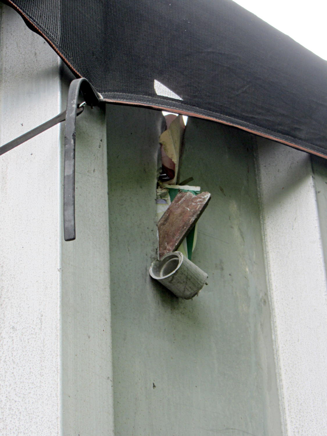
The trailer also had several puncture wounds:
Metal scrap trailer – Puncture wounds
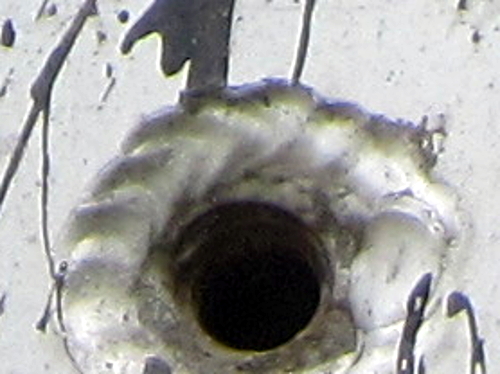
I didn’t notice the circular feature at the bottom center until I looked at the picture, but it certainly reminded me of a bullet hole in glass plate. Close inspection of the original image suggests it’s a welded stress relief border around a drilled hole, perhaps with a boss on the inside of the trailer:
Lining the shield support box with copper foil tape turned out to be surprisingly easy:
Electrometer amp – shield – end view
The flat surface is two overlapping strips of 2 inch wide copper tape. I traced the exterior of the support box on the tape, cut neatly along the lines, slit the corners, bent the edges upward, peeled off the backing paper, stuck the tape into the box, pressed the edges into the corners, and didn’t cut myself once.
Applying 1 inch wide tape to the wall went just as smoothly, after I realized that I should cut it into strips just slightly longer than the hexagon’s sides.
The tape along the rim is adhesive copper mesh that’s springy enough to make contact all around the edge. I cut the 1 inch wide tape in half, which was just barely wide enough to reach::
Electrometer amp – shield – mesh soldering
Although you’re supposed to join the entire length of each seam for best RF-proofing, I tacked the corners and the middle of the long edge, then hoped for the best. The copper mesh seems to be plated on plastic threads that requires a fast hand to solder without melting, but I’m getting better at it. The adhesive is said to be conductive, but I loves me some good solder blob action.
The resistance from the flat bottom to the side panels and the fabric on the edge started out at a few ohms before soldering and dropped to 0.0 Ω after soldering, so I’ll call it a success. Didn’t even melt the outside of the PETG box, but I admit I didn’t take it apart to see what the copper-to-PETG surface looks like.
Covering the foil on the sides with 1 inch Kapton tape completed the decoration. I didn’t bother to cover the flat surface, because none of the circuitry should reach that far, and didn’t worry about covering the fabric tape for similar reasons. As madbodger pointed out, this violates the no-plastic-on-the-inside rule, but I’m still hoping for better results than having the entire plastic structure with all its charges on the inside.
A strip of horribly clashing orange plastic tape (which might be splicing tape for reel-to-reel recording tape) covers the outside edges of the fabric, prevents fraying, and gives the black electrical tape that holds the box down a solid grip:
Electrometer amp – shield – exterior
Yeah, like you’d notice mismatched colors around here.
Using black tape as an anchor seemed easier and better than messing with nesting pins & sockets. The copper fabric tape makes good contact with the rim of the PCB all the way around the perimeter and the black tape holds it firmly in place.
Early reports suggest the shield works pretty well…
Although I’d thought of a Mu-metal shield, copper foil tape should be easier and safer to shape into a simple shield. The general idea is to line the interior with copper tape, solder the joints together, cover with Kapton tape to reduce the likelihood of shorts, then stick it in place with some connector pin-and-socket combinations. Putting the tape on the outside would be much easier, but that would surround the circuitry with a layer of plastic that probably carries enough charge to throw things off.
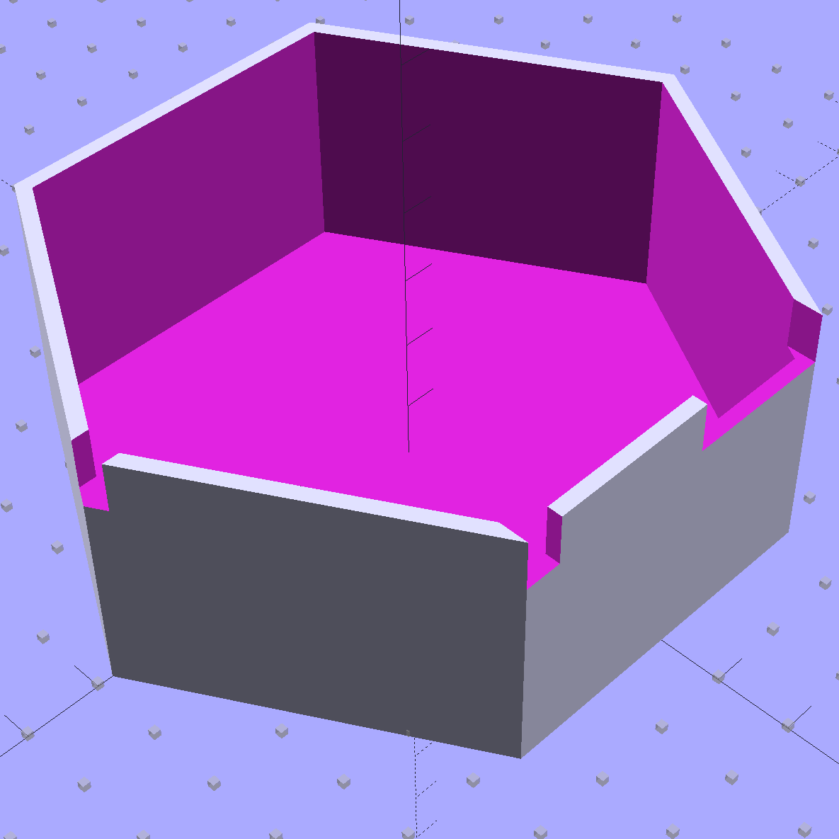
Anyhow, the hexagonal circuit board model now sports a hexagonal cap to support the shield:
Victoreen 710-104 Ionization Chamber Fittings – Show with shield
The ad-hoc openings fit various switches, wires, & twiddlepots:
If white LED strips had existed in the early 1980s, the engineers responsible for the HP 7475A plotter would surely have done this:
HP 7475A Plotter – LED paper illumination
Not, that’s not stretched vertically: I bought a ream of B-size paper (11×17 inches) just for plotter demos.
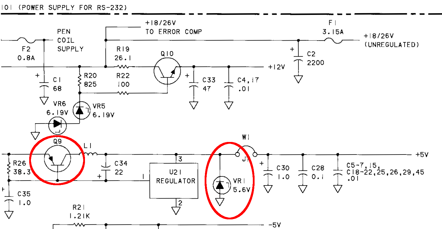
Although the power supply does have a +12 V output, it comes from a TO220 transistor without a heatsink. The +5 V supply uses a robust TO3 transistor on a huge quad heatsink that can surely dissipate another watt or two without getting any sweatier.
I powered the LEDs from a dirt-cheap boost converter that provides a convenient brightness adjustment; it’s set to 10.5 V and that’s plenty bright enough. The converter attaches to pair of wires soldered across VR1, which is probably a crowbar that blows F3 (not shown) in the event the regulator fails hot:
HP 7475A – LED power tap – schematic
They don’t make power supplies like that any more.
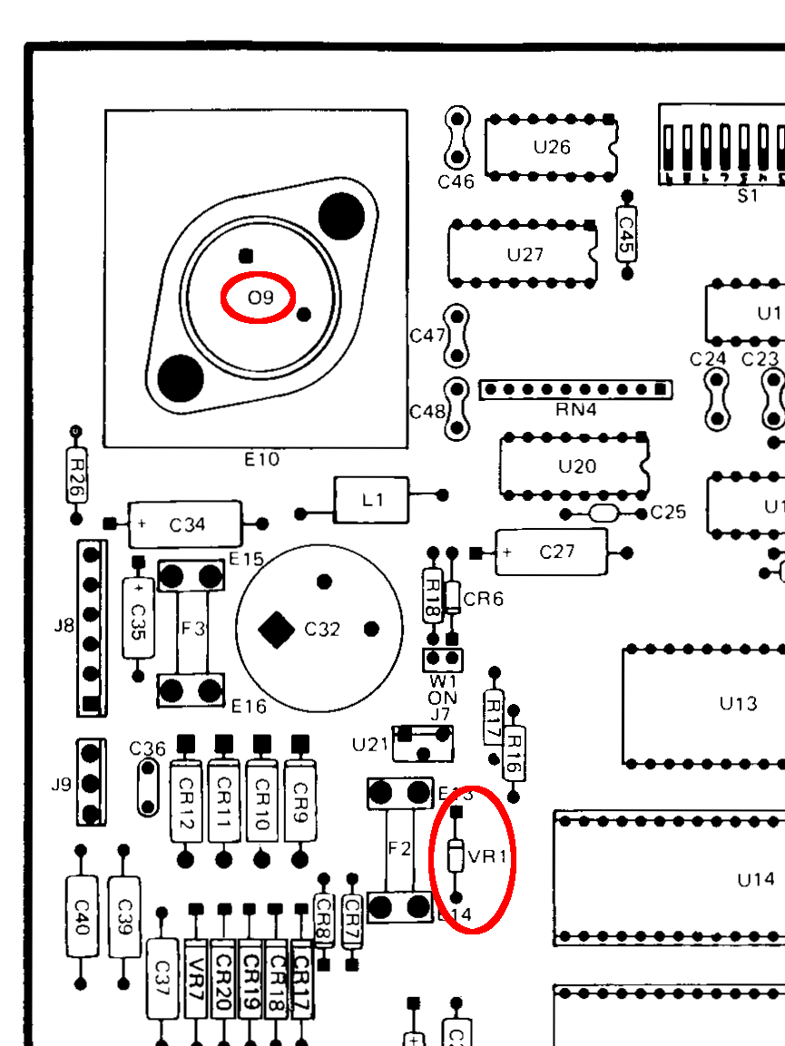
The part locations (“O9” looks like a typo):
HP 7475A – LED power tap
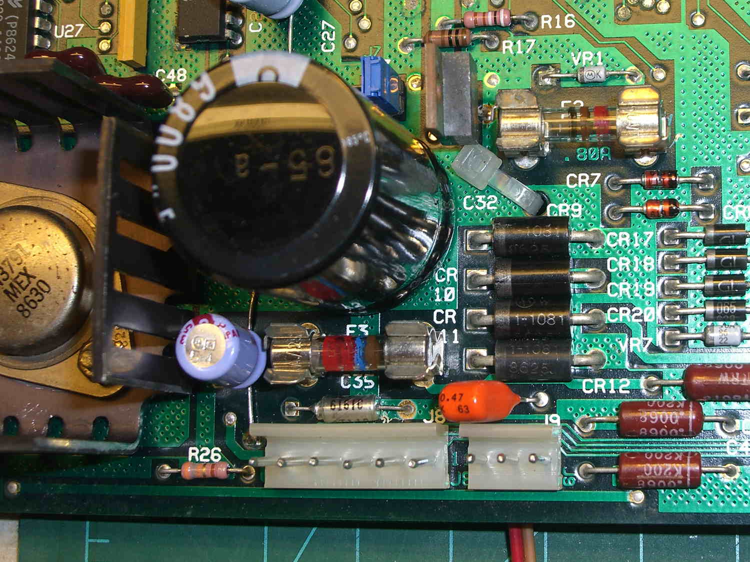
The PCB has holes in exactly the right spot for a zip tie anchoring the wires exiting to the bottom:
HP 7475A Plotter – LED power tap – PCB top
This vertiginous view shows the inside of the case atop the chassis, with the boost converter affixed to the galvanized steel pan with foam tape and the LED wires stuck down with Gorilla Tape:
HP 7475A Plotter – LED strip and boost converter
Red silicone tape around a PCB-mount coax jack rounds out a true hack job.
Although I didn’t bring the plotter to the CNC Workshop, that venue’s dim light reminded me that you can never have enough light when you’re showing off your toys: the LED panels on the M2 and the LED light bars on the Model 158 sewing machine were the brightest spots to be seen.
Imagine “updating” these windows with modern high-efficiency glass:
Terwilliger House – parallelogram windows
That’s the end wall of the 1738 Terwilliger House on the Locust Lawn site. I’m sure the woodwork doesn’t date back that far, but the glazier demonstrated genius-level mastery.
We were on a fascinating behind-the-scenes tour, marred by a visitor who knew the rules about not touching the exhibits didn’t apply to her. My parents ran a restaurant / gift shop and, to this day, my hands automatically find their way into my pockets when I enter a store, let alone a museum.
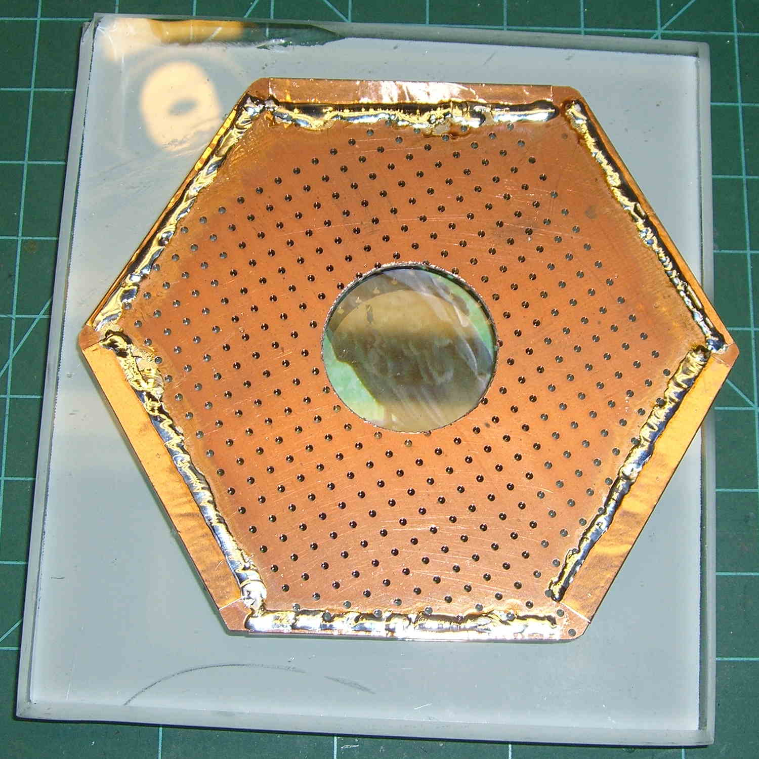
Just to have something to work with, I cut a hex from a sheet of double-sided PCB stock and bonded the edges with copper foil:
Victoreen 710-104 – Hex PCB – top
Slightly wider tape on three edges will clear the board supports:
Victoreen 710-104 – Hex PCB – bottom
For unknown reasons, the PCB has arrays of plated-through holes firmly bonding the top and bottom copper, so that’s pretty much solid copper with a glass-epoxy core. I think somebody (else) harvested it from a locally important company many, many decades ago, but it arrived with no provenance.
The first pass at the electrometer circuitry will be air-wired for low leakage, which is pretty much the only way I have to actually get low leakage; the holes should help glue the parts to that copper plane.
I’m not at all convinced the big hole in the middle is strictly necessary. The chamber has 10 pF from pin to can that should swamp any stray capacitance unless I do something really stupid.
Given my weak origami-fu and the need for hexagonality, I should print a 3D template.
It’s worth remembering that both the hex and the shield will be at the can’s +24 V potential, not “ground”. That makes no difference to the external circuitry, but will certainly cause me to blow a few junctions along the way.
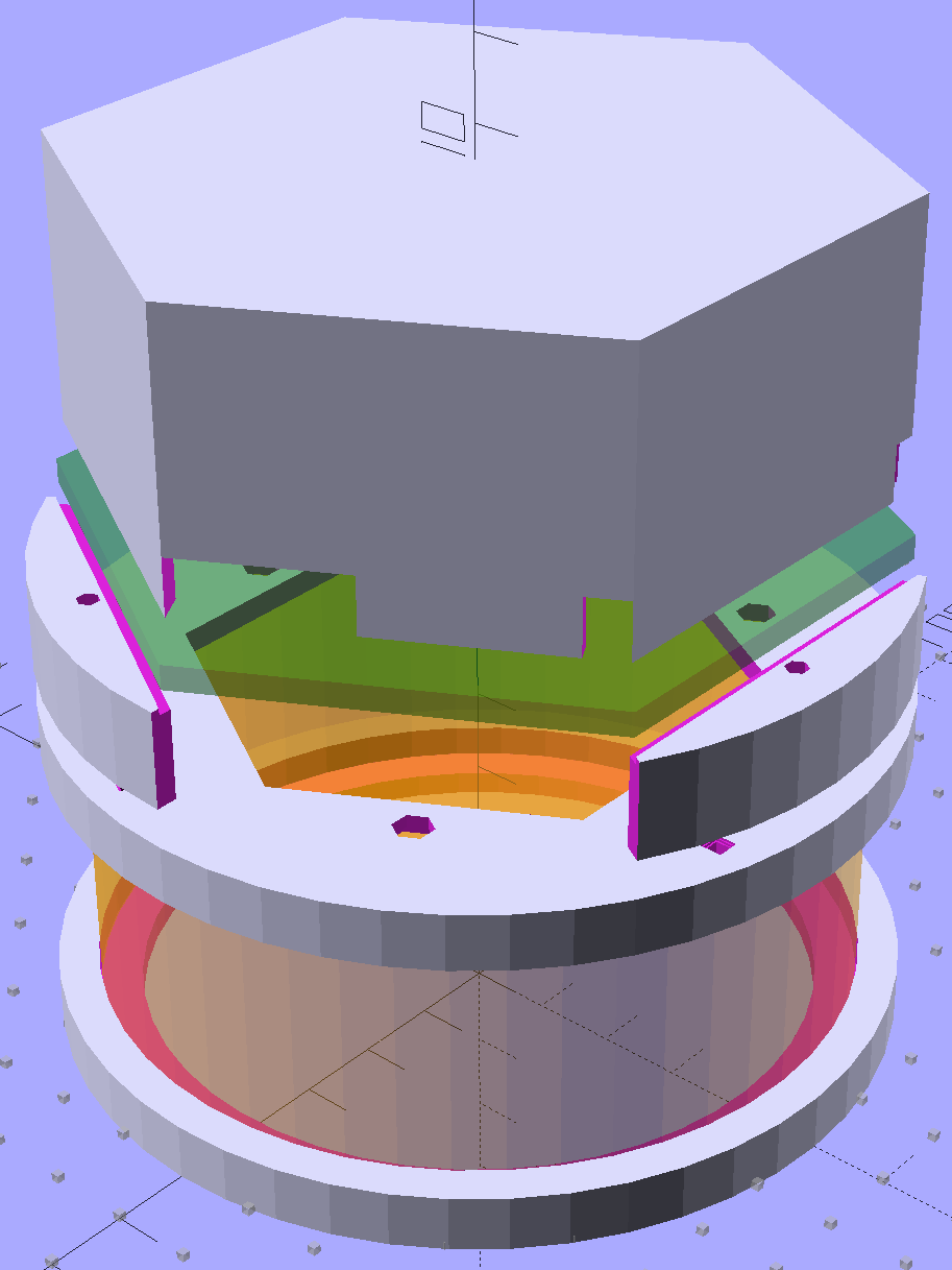
The general idea is to put the electrometer circuitry directly atop the Victoreen 710-104 ionization chamber, so as to minimize the distance from the center collector electrode to the electrometer input. After a few false starts, this looked promising:
Victoreen 710-104 Ionization Chamber Fittings – Show layout
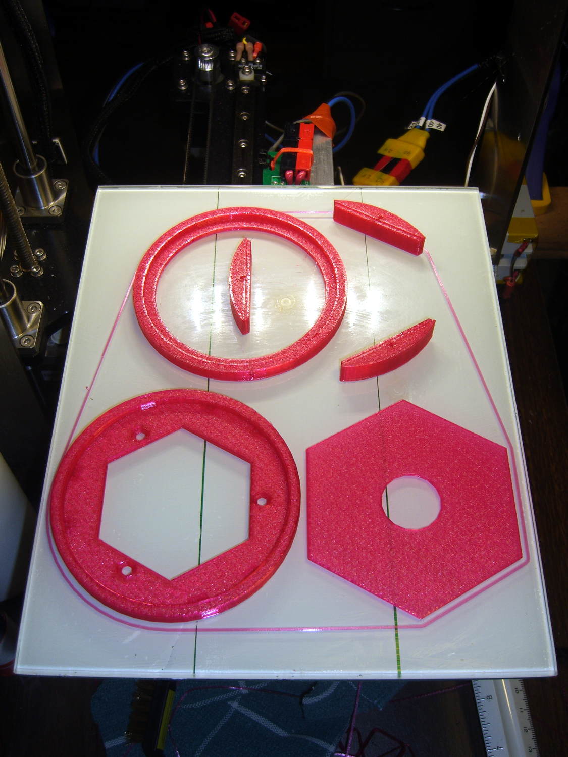
The hexagonal circuit board fits the can so nicely that I’ll run with it, despite the over-the-top twee factor. Because it’s so hard to freehand a hex, I printed the green object as a tracing template, despite having the Slic3r preview show the parts just barely fitting on the M2 platform:
The skirt measures 0.25±0.05 around the entire perimeter, with a slight positive bias (platform too low) along the left side and a corresponding negative bias on the right. Both sides look just fine to me.
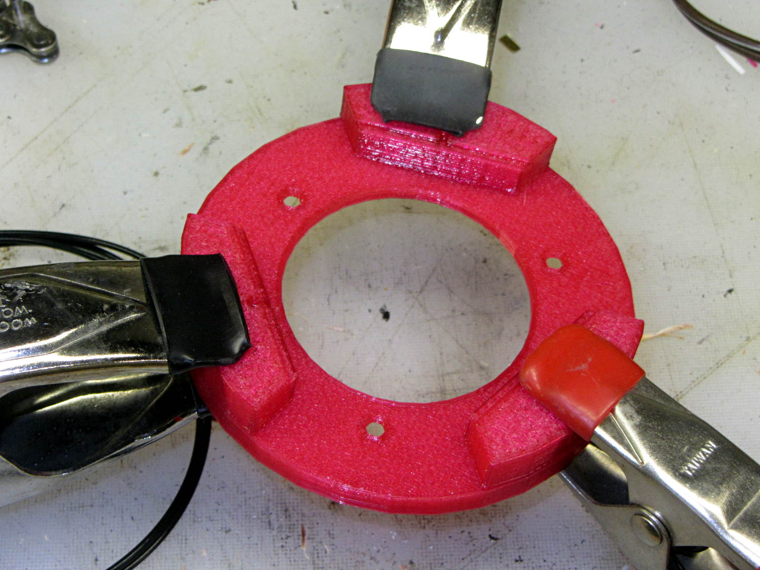
A pair of alignment pegs hold each board support in place while gluing:
Victoreen 710-104 Fittings – clamping
Next time around, I’ll glue the supports with the circuit board template laid in place to ensure the edges have the proper orientation, but they came out surprisingly close just by matching the outer perimeters. Of course, I probably bandsawed / belt sanded the carefully traced hex just slightly off-kilter.
The outer perimeter has 48 sides. Making it a multiple of three means each board support has the same pattern of sides and all will be interchangeable. Making it a multiple of four means each quadrant has the same pattern of sides and the ring looks pleasingly symmetrical. The factor-of-three is most important: you want interchangeable supports. Trust me on this.
The bottom ring keeps the solder dimple that seals the can base off the desk, but I also stuck a quartet of rubber feet on the can for better traction.
Here’s what it looks like with the two A23 12 V bias batteries in their holders, affixed to the can with foam tape:
Victoreen 710-104 Fittings – assembled
The OpenSCAD source code includes a few more tweaks:
// Victoreen 710-104 Ionization Chamber Fittings
// Ed Nisley KE4ZNU July 2015

Layout = "Show";
					// Show - assembled parts
					// Build - print them out!
					// CanCap - PCB insulator for 6-32 mounting studs
					// CanBase - surrounding foot for ionization chamber
					// CanLid - generic surround for either end of chamber
					// PCB - template for cutting PCB sheet
					// PCBBase - holder for PCB atop CanCap

BuildTemplate = false;			// true to build PCB template along with everything else

//- Extrusion parameters must match reality!
//  Print with 2 shells and 3 solid layers

ThreadThick = 0.25;
ThreadWidth = 0.40;

HoleWindage = 0.2;

Protrusion = 0.1;			// make holes end cleanly

AlignPinOD = 1.75;			// assembly alignment pins = filament dia

inch = 25.4;

function IntegerMultiple(Size,Unit) = Unit * ceil(Size / Unit);

//- Screw sizes

Tap4_40 = 0.089 * inch;
Clear4_40 = 0.110 * inch;
Head4_40 = 0.211 * inch;
Head4_40Thick = 0.065 * inch;
Nut4_40Dia = 0.228 * inch;
Nut4_40Thick = 0.086 * inch;
Washer4_40OD = 0.270 * inch;
Washer4_40ID = 0.123 * inch;


//----------------------
// Dimensions

OD = 0;											// name the subscripts
LENGTH = 1;

Chamber = [91.0 + HoleWindage,38];				// Victoreen ionization chamber dimensions

Stud = [										// stud welded to ionization chamber lid
	[6.5,IntegerMultiple(0.8,ThreadThick)],		// flat head -- generous clearance
	[4.0,9.5],									// 6-32 screw -- ditto
];
NumStuds = 3;
StudSides = 6;									// for hole around stud

BCD = 2.75 * inch;								// mounting stud bolt circle diameter

PlateThick = 3.0;								// layer atop and below chamber ends
RimHeight = 4.0;								// extending up along chamber perimeter
WallHeight = RimHeight + PlateThick;
WallThick = 5.0;								// thick enough to be sturdy & printable
CapSides = 8*6;									// must be multiple of 4 & 3 to make symmetries work out right

PCBFlatsOD = 85.0 + 2*ThreadWidth;				// hex dia across flats + clearance
PCBThick = 1.1;
PCB = [PCBFlatsOD / cos(30),PCBThick - ThreadThick];		// OD = tip-to-tip dia

echo(str("Actual PCB across flats: ",PCBFlatsOD - 2*ThreadWidth));
echo(str(" ... tip-to-tip dia: ",(PCBFlatsOD - 2*ThreadWidth)/cos(30)));
echo(str(" ... thickness: ",PCBThick));

HolderHeight = 11.0 + PCB[LENGTH];				// thick enough for PCB to clear studs
HolderShelf = 2.0;								// shelf under PCB edge

echo(str("PCB holder height: ",HolderHeight));
echo(str(" ... across flats: ",PCBFlatsOD));

//----------------------
// Useful routines

module PolyCyl(Dia,Height,ForceSides=0) {			// based on nophead's polyholes

  Sides = (ForceSides != 0) ? ForceSides : (ceil(Dia) + 2);

  FixDia = Dia / cos(180/Sides);

  cylinder(r=(FixDia + HoleWindage)/2,
           h=Height,
	   $fn=Sides);
}

//- Locating pin hole with glue recess
//  Default length is two pin diameters on each side of the split

module LocatingPin(Dia=AlignPinOD,Len=0.0) {

	PinLen = (Len != 0.0) ? Len : (4*Dia);

	translate([0,0,-ThreadThick])
		PolyCyl((Dia + 2*ThreadWidth),2*ThreadThick,4);

	translate([0,0,-2*ThreadThick])
		PolyCyl((Dia + 1*ThreadWidth),4*ThreadThick,4);

	translate([0,0,-Len/2])
		PolyCyl(Dia,Len,4);

}

module ShowPegGrid(Space = 10.0,Size = 1.0) {

  RangeX = floor(100 / Space);
  RangeY = floor(125 / Space);

	for (x=[-RangeX:RangeX])
	  for (y=[-RangeY:RangeY])
		translate([x*Space,y*Space,Size/2])
		  %cube(Size,center=true);
}

//-----

module CanLid() {

	difference() {
		cylinder(d=Chamber[OD] + 2*WallThick,h=WallHeight,$fn=CapSides);
		translate([0,0,PlateThick])
			PolyCyl(Chamber[OD],Chamber[1],CapSides);
	}

}

module CanCap() {

	difference() {
		CanLid();

		translate([0,0,-Protrusion])											// central cutout
//			cylinder(d=(BCD - 2*5.0),h=Chamber[LENGTH],$fn=CapSides);
			rotate(180/6)
				cylinder(d=BCD,h=Chamber[LENGTH],$fn=6);

		for (i=[0:(NumStuds - 1)])												// stud clearance holes
			rotate(i*360/NumStuds)
				translate([BCD/2,0,0])
					rotate(180/StudSides) {
						translate([0,0,(PlateThick - (Stud[0][LENGTH] + 2*ThreadThick))])
							PolyCyl(Stud[0][OD],2*Stud[0][LENGTH],StudSides);
						translate([0,0,-Protrusion])
							PolyCyl(Stud[1][OD],2*Stud[1][LENGTH],StudSides);
					}

		for (i=[0:(NumStuds - 1)], j=[-1,1])									// PCB holder alignment pins
			rotate(i*360/NumStuds + j*15 + 60)
				translate([Chamber[OD]/2,0,0])
					rotate(180/4)
						LocatingPin(Len=2*PlateThick - 2*ThreadThick);
	}

}

module CanBase() {

	difference() {
		CanLid();
		translate([0,0,-Protrusion])
			PolyCyl(Chamber[OD] - 2*5.0,Chamber[1],CapSides);
	}
}

module PCBTemplate() {

	difference() {
		cylinder(d=((PCBFlatsOD - 2*ThreadWidth)/cos(30)),h=max(PCB[LENGTH],3.0),$fn=6);		// actual PCB size, overly thick
		translate([0,0,-Protrusion])
			cylinder(d=10,h=10*PCB[LENGTH],$fn=12);
	}
}

module PCBBase() {

	difference() {
		cylinder(d=Chamber[OD] + 2*WallThick,h=HolderHeight,$fn=CapSides);

		rotate(30) {
			translate([0,0,-Protrusion])										// central hex
				cylinder(d=(PCBFlatsOD - 2*HolderShelf)/cos(30),h=2*HolderHeight,$fn=6);

			translate([0,0,HolderHeight - PCB[LENGTH]])							// hex PCB recess
				cylinder(d=PCB[OD],h=HolderHeight,$fn=6);

			for (i=[0:NumStuds - 1])											// PCB retaining screws
				rotate(i*120 + 30)
					translate([(PCBFlatsOD/2 + Clear4_40/2 + ThreadWidth),0,-Protrusion])
						rotate(180/6)
							PolyCyl(Tap4_40,2*HolderHeight,6);

			for (i=[0:(NumStuds - 1)], j=[-1,1])								// PCB holder alignment pins
				rotate(i*360/NumStuds + j*15 + 30)
					translate([Chamber[OD]/2,0,0])
						rotate(180/4)
							LocatingPin(Len=PlateThick);
		}

		for (i=[0:NumStuds - 1])												// segment isolation
			rotate(i*120 - 30)
				translate([0,0,-Protrusion]) {
					linear_extrude(height=2*HolderHeight)
						polygon([[0,0],[Chamber[OD],0],[Chamber[OD]*cos(60),Chamber[OD]*sin(60)]]);
				}
	}


}


//----------------------
// Build it

ShowPegGrid();

if (Layout == "CanLid") {
	CanLid();
}

if (Layout == "CanCap") {
	CanCap();
}

if (Layout == "CanBase") {
	CanBase();
}

if (Layout == "PCBBase") {
	PCBBase();
}

if (Layout == "PCB") {
	PCBTemplate();
}

if (Layout == "Show") {
	CanBase();
	color("Orange",0.5)
		translate([0,0,PlateThick + Protrusion])
			cylinder(d=Chamber[OD],h=Chamber[LENGTH],$fn=CapSides);
	translate([0,0,(2*PlateThick + Chamber[LENGTH] + 2*Protrusion)])
		rotate([180,0,0])
			CanCap();
	translate([0,0,(2*PlateThick + Chamber[LENGTH] + 5.0)])
		PCBBase();
	color("Green",0.5)
		translate([0,0,(2*PlateThick + Chamber[LENGTH] + 7.0 + HolderHeight)])
			rotate(30)
				PCBTemplate();
}

if (Layout == "Build") {

	if (BuildTemplate) {
		translate([-0.50*Chamber[OD],-0.60*Chamber[OD],0])
			CanCap();

		translate([0.55*Chamber[OD],-0.60*Chamber[OD],0])
			rotate(30)
				PCBTemplate();
	}
	else {
		translate([-0.25*Chamber[OD],-0.60*Chamber[OD],0])
			CanCap();
	}

	translate([-0.25*Chamber[OD],0.60*Chamber[OD],0])
		CanBase();
	translate([0.25*Chamber[OD],0.60*Chamber[OD],0])
		PCBBase();
}