Ed Nisley's Blog: Shop notes, electronics, firmware, machinery, 3D printing, laser cuttery, and curiosities. Contents: 100% human thinking, 0% AI slop.
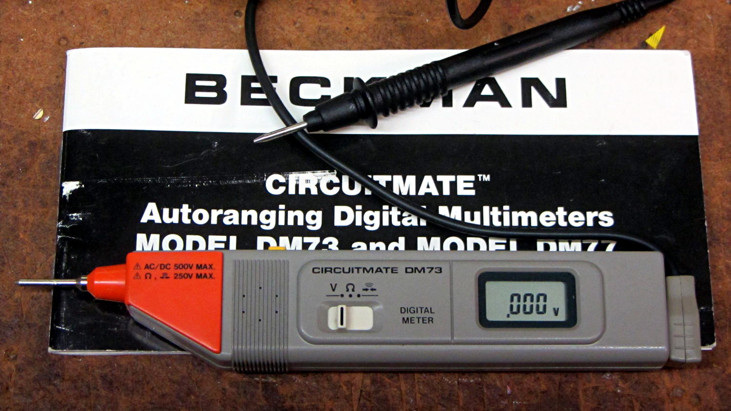
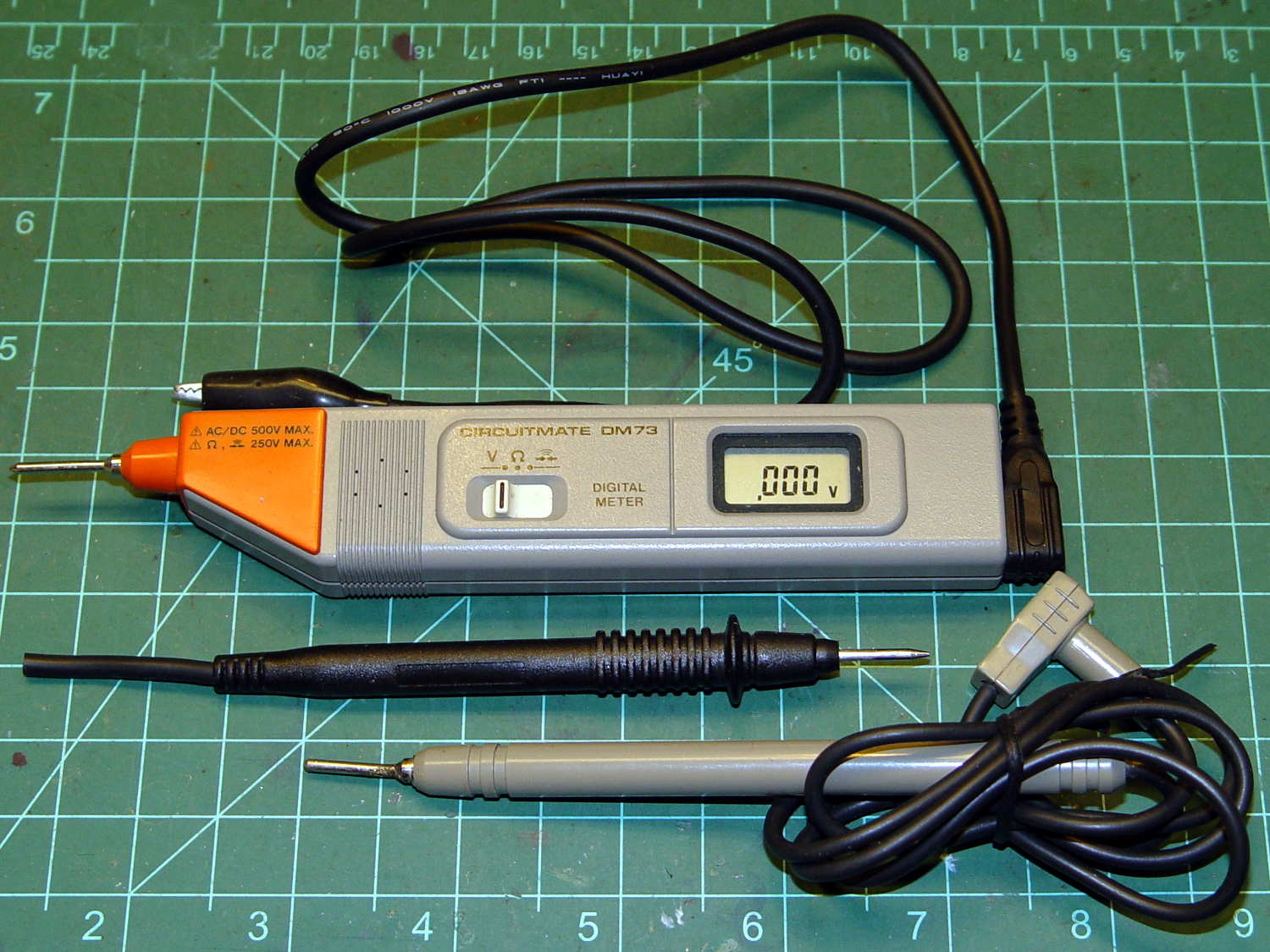
Prompted by the condolences on the death of my Beckman DM73 Circuitmate, I brought the carcass back to Squidwrench, took it apart, annoyed the switches, and re-soldered the battery connections:
Beckman DM73 Circuitmate – restored
I worked minute dots of Caig DeoxIT into the switches, without disassembling them, with magical thinking guiding my technique. One of the battery connections seemed suspect, but we’ll never know.
In any event, it beeps happily when turned on (*), the LCD behaves properly, it’s no longer pressure-sensitive, and life is good! It surely needs calibration, but that’s definitely in the nature of fine tuning.
Thanks for nudging me into Doing The Right Thing™.
(*) Including the double beep with the AC/DC button held down.
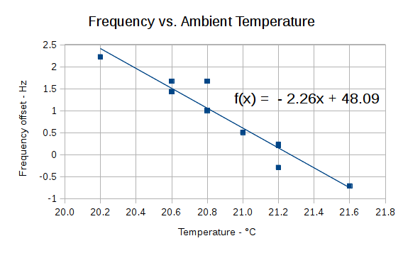
While tinkering with the SPI code for the AD9850 DDS module, I wrote down the ambient temperature and the frequency tweak required to zero-beat the 10 MHz output with the GPS-locked oscillator. A quick-n-dirty plot summarizing two days of randomly timed observations ensued:
AD9850 DDS Module – Frequency vs Temperature
The frequency offset comes from the tweak required to zero-beat the output by adjusting the initial oscillator error: a positive tweak produces a smaller count-per-hertz coefficient and reduces the output frequency. As a result, the thermal coefficient sign is backwards, because increasing temperature raises the oscillator frequency and reduces the necessary tweak. I think so, anyway; you know how these things can go wrong. More automation and reliable data would be a nice touch.
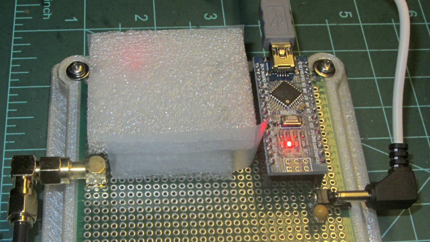
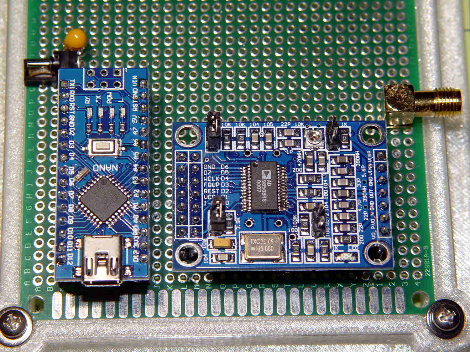
Foam sheets formed a block around the DDS module, isolating it from stray air currents and reducing the clock oscillator’s sensitivity:
AD9850 DDS module – foam insulation
I used the ambient temperature, because the thermocouple inside the foam (not shown in the picture) really wasn’t making good contact with the board, the readings didn’t make consistent sense, and, given a (nearly) constant power dissipation, the (average) oscillator temperature inside the foam should track ambient temperature with a constant offset. I think so, anyway.
The coefficient works out to 0.02 ppm/°C. Of course, the initial frequency offset is something like -400 Hz = 3 ppm, so we’re not dealing with lab-grade instrumentation here.
Spoiler alert: having spent a while trying to fit the DDS calculations into fixed-point numbers stuffed into a single 32 bit unsigned long value, it’s just a whole bunch of nope.
The basic problem, as alluded to earlier, comes from calculations on numbers near 32768.0 and 60000.0 Hz, which require at least 6 significant digits. Indeed, 0.1 Hz at 60 kHz works out to 1.7 ppm, so anything around 0.05 Hz requires seven digits.
The motivation for fixed-point arithmetic, as alluded to earlier, comes from the amount of program memory and RAM blotted up by the BigNumber arbitrary precision arithmetic library, which seems like a much bigger hammer than necessary for this problem.
So, we begin.
Because the basic tuning increment works out to 0.0291 Hz, you can’t adjust the output frequency in nice, clean 0.01 Hz clicks. That doesn’t matter, as long as you know the actual frequency with some accuracy.
Setting up the DDS requires calculations involving numbers near 125.000000 MHz and 2³², both of which sport nine or ten significant figures, depending on how fussy you are about calibrating the actual oscillator frequency and how you go about doing it. Based on a sample of one AD8950 DDS board, the 125 MHz oscillator runs 300 to 400 Hz below its nominal 125 MHz: about 3 ppm low, with a -2.3 Hz/°C tempco responding to a breath. It’s obviously not stable enough for precise calibration, but even 1 ppm = 125 Hz chunks seem awkwardly large.
Many of the doodles below explore various ways to fit integer values up to 125 MHz and fractions down to 0.0291 Hz/count into fixed point numbers with 24 integer bits + 8 fraction bits, perhaps squeezed a few bits either way. Fairly obviously, at least in retrospect, it can’t possibly work: 125×10⁶ requires 28 bits. Worse, 8 fraction bits yield steps of 0.0039, so you start with crappy resolution.
The DDS tuning word is about 2×10⁶ for outputs around 60 kHz, barely covered by 21 bits. You really need at least seven significant figures = 0.1 ppm for those computations, which means the 125 MHz / 2³² ratio must carry seven significant figures, which means eight decimal places: 0.02910383 and not a digit less.
En passant, it’s disturbing how many Arduino DDS libraries declare all their variables as double and move on as if the quantities were thereby encoded in 64 bit floating point numbers. Were that the case, I’d agree 125e6 / pow(2.0,32) actually meant something, but it ain’t so.
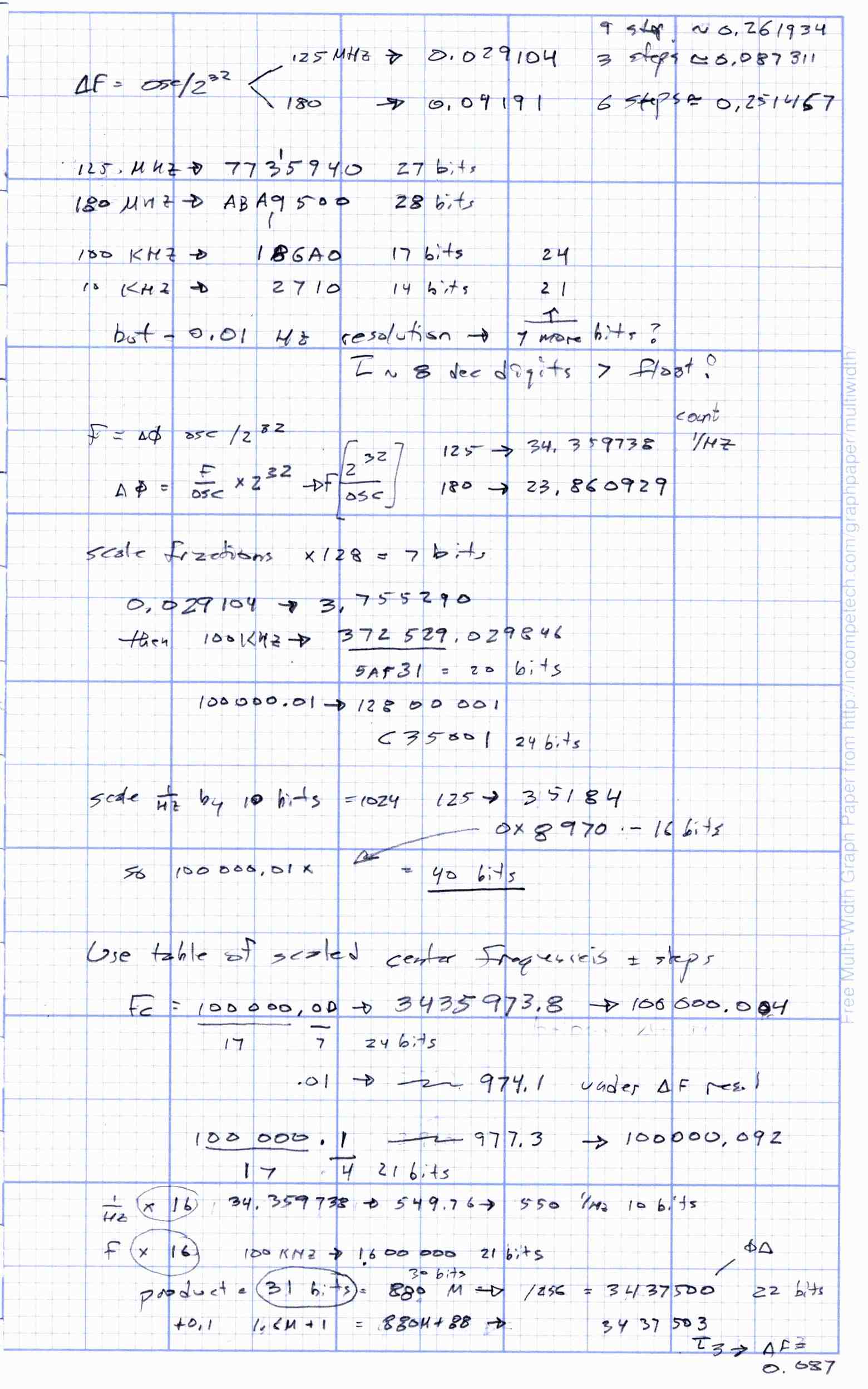
The original non-linear doodles, which, despite containing some values useful in later computations, probably aren’t worth your scrutiny:
AD9850 DDS Fixed-point Number Doodles – 1AD9850 DDS Fixed-point Number Doodles – 2AD9850 DDS Fixed-point Number Doodles – 3AD9850 DDS Fixed-point Number Doodles – 4AD9850 DDS Fixed-point Number Doodles – 5AD9850 DDS Fixed-point Number Doodles – 6AD9850 DDS Fixed-point Number Doodles – 7AD9850 DDS Fixed-point Number Doodles – 8
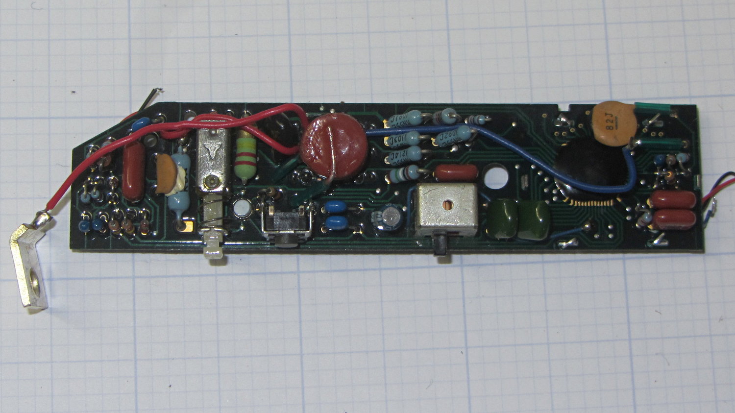
I’d added Mad Phil’s trusty Circuitmate to the tool kit I carry along to Squidwrench:
Beckman DM73 – new ground clip
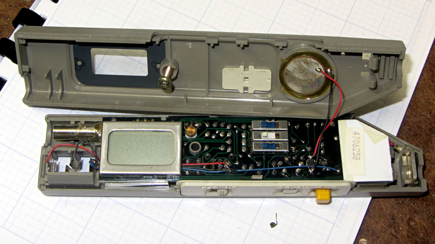
Over the last few months it became increasingly erratic, eventually got to the point where slight pressure on the case would blank the display, and finally didn’t turn on at all. Yes, I replaced the batteries.
So I took it apart:
Beckman DM73 Circuitmate – case open
Nothing seemed particularly broken and, even after resoldering all the joints, it continued to not work at all:
Beckman DM73 Circuitmate – PCB
If you want to try your hand at instrument rehabilitation, let me know.
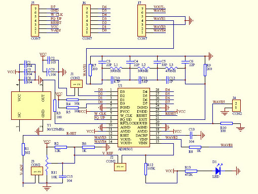
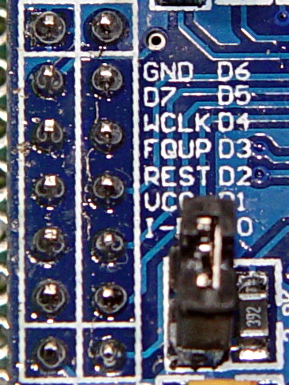
… with any of the doc for the generic AD8950/51 DDS modules you’ll find out on the Interwebs. This snippet from the seller’s schematic will suffice:
AD9850 module schematic – cropped
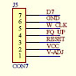
Here’s a closer look at the 2×7 header in the upper left corner:
AD9850 module schematic – J5 detail
Don’t blame me for the blur, the schematic is a JPG.
Compared it with the board in hand:
AD9850 DDS Module – swapped GND D7 pins – detail
Yup, the D7 and GND pins are reversed.
Some careful probing showed the silkscreen is correct: the pins are, in fact, correctly labeled.
Should you be laying out a PCB in the expectation of using any DDS module from the lowest-price supplier, remember this high truth: Hell hath no fury like that of an unjustified assumption.
Fortunately, I’m hand-wiring the circuit and caught it prior to the smoke test.
Adding a 56 nF cap across the C6 terminals (just above the AD8310) lowered the VBW to about 1 kHz:
AD8310 Log Amp module – VBW rolloff cap
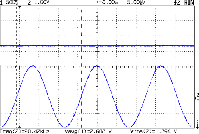
Which flattened that sucker right out:
AD8310 – 1 kHz VBW cap – 60 kHz 1.394 V
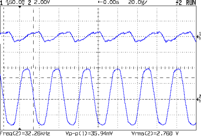
The ripple for an absurdly high amplitude 32 kHz signal amounts to 36 mV:
AD8310 – 1 kHz VBW cap – 32 kHz – VBW ripple
Firing the tracking generator into the input with a frequency sweep from 100 kHz to 250 MHz shows the low end looks much better:
AD8310 – 1 kHz VBW cap – 100 kHz 250 MHz – 0 dB atten
There’s a slight droop across the sweep that might amount to 50 mV = 2 dB, which I’m inclined to not worry about in this context.
Applying the attenuators once again produces a scale factor of 23.5 mV/dB across 30 dB of RF, but this time the 60 kHz output makes sense, too.
Using the typical output curve from AN-691, that 2.0 V output corresponds to -13 dBm, which sounds about right for the tracking generator (which might really be -10 dBm).
I must calibrate the log amp output to find the actual intercept point (nominally -95 dBm, but could range from -86 to -102) at 60 kHz. The intercept is the extrapolated RF input producing 0 V out, which then acts as an offset for the voltage-to-dBm calculation; you start by finding the slope of the voltage vs. dBm line at some convenient power levels, then solve for dBm with V=0.
So a cheap AD8310 Log Amp module from eBay can work in the LF band, after you rearrange the input circuitry and tweak the chip’s filters. At least now I have a better understanding of what’s going on …
Given the intended LF crystal-measurement application, a hulking 51 Ω metal film resistor sprawled across the ground plane will work just fine. All three ceramic caps measure a bit under 1 µF; I intended to solder the input caps atop the existing 10 nF caps, but that didn’t work out well at all.
I should harvest the InLo SMA connector to prevent anyone from mistaking it for an actual input.
With that in place, the log amp output makes more sense:
AD8310 – modified – 100 kHz 150 MHz – 0 dB atten
That trace tops out at 150 MHz, not the previous 500 MHz, but now the response is flat all the way out. The log amp generates plenty of hash when the tracking generator isn’t producing a valid signal.
The 60 kHz response looks different:
AD8310 – modified – 60 kHz 1Vpp
So it’s really the log amp response to the absolute value of the sine wave (or, more accurately, to the sine wave re-zeroed around Vcc/2), with minimum output at the input’s zero crossings. At 500 mV/div, the log amp says the input varies by 42 dB = 1000 mV/(24 mV/dB), which might actually be about right for a zero-crossing (or zero-approaching absolute value of a) signal; logarithms don’t deal well with zeros.
The AD8310 datasheet and AN-691 suggest the 2.5 V output corresponds to +10 dBm = 12.5 Vrms input, which flat-out isn’t the case. However, the actual 500 mVpeak = 350 mVrms input is 2.5 mW = +4 dBm, so maybe it’s within spitting distance of being right.
AN-691 recommends 10 µF input caps for “low frequency” use, showing results down to 20 Hz; 1 µF seems to get the circuit close enough to the goal for use near 60 kHz.
It also recommends a cap on the BFIN pin (pin 6) to reduce the output stage bandwidth = “video bandwidth” and improve the overall accuracy, which remains to be done. The datasheet suggests rolling VBW off at 1/10 the minimum input frequency, which would be around 3 kHz for use with 32.768 kHz crystals. The equation, with reference to the internal 3 kΩ bias resistor:
CFILT = 1/(2π 3 kΩ VBW) – 2.1 pF = 18 nF
For a bit more margin, 1 kHz would require 56-ish nF.
The PCB has a convenient pair of pads labeled C6 for that capacitor. This may require protracted rummaging in the SMD capacitor stash.
Rolling off the VBW should reduce the hash on the 100 kHz end of the frequency sweep and filter the 60 kHz response down to pretty much a DC level.
Applying the 10 dB and 20 dB SMA attenuators to the input from the tracking generator and recording the log amp output voltage produces this useful table:
AD8310 Log Amp – mods and log response
With the terminating resistor on the correct side of the input caps, the log amp seems to be working the way it should, with an output varying a bit under the nominal 24-ish mV/dB over a 30 dB range.
We need caps! Lots of caps!
A quick search with the obvious keywords suggests nobody else has noticed how these modules work over a reasonable bandwidth. Maybe I’m the first person to use them in the LF band?