The Smell of Molten Projects in the Morning

Ed Nisley's Blog: Shop notes, electronics, firmware, machinery, 3D printing, laser cuttery, and curiosities. Contents: 100% human thinking, 0% AI slop.

Author: Ed

  • Measuring Objects for 3D Modeling: USB Video Camera

    A brace of “Fashion” USB video cameras arrived from halfway around the planet. According to the eBay description and the legend around the lens, they’re “5.0 Megapixel”:

    Fashion USB camera - case front
    Fashion USB camera – case front

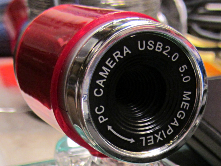
    The reality, of course, is that for five bucks delivered you get 640×480 VGA resolution at the hardware level and their Windows driver interpolates the other 4.7 megapixels. VGA resolution will be good enough for my simple needs, particularly because the lens has a mechanical focus adjustment; the double-headed arrow symbolizes the focus action.

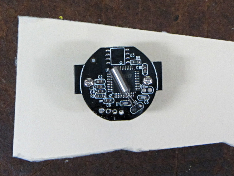
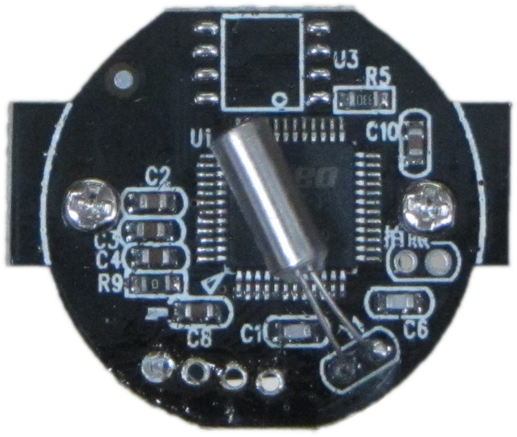
    But the case seemed entirely too bulky and awkward. A few minutes with a #0 Philips screwdriver extracted the actual camera hardware, which turns out to be a double-sided PCB with a lens assembly on the front:

    Fashion USB video - case vs camera
    Fashion USB video – case vs camera

    The PCB has asymmetric tabs that ensure correct orientation in the case:

    Fashion USB camera - wired PCB rear
    Fashion USB camera – wired PCB rear

    In order to build an OpenSCAD model for a more compact case, we need the dimensions of that PCB and those tabs…

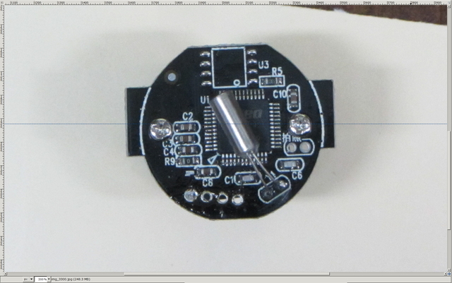
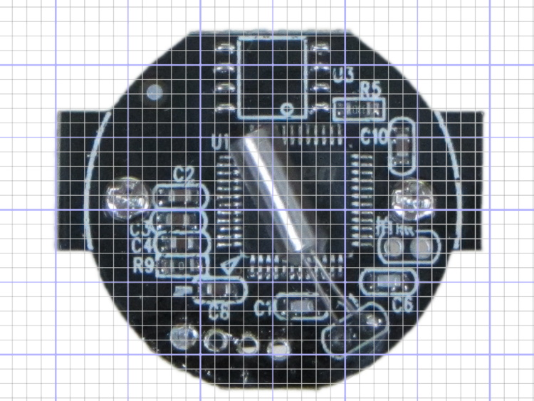
    Start with a picture of the back of the PCB against white paper, taken from a few feet to flatten the perspective:

    img_3300 - Camera PCB on white paper
    img_3300 – Camera PCB on white paper

    Load it into The GIMP, zoom in, and pull a horizontal guide line down to about the middle of the image:

    Camera PCB - horizontal guide - scaled
    Camera PCB – horizontal guide – scaled

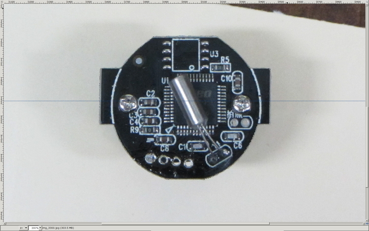
    Rotate to align the two screws horizontally (they need not be centered on the guide, just lined up horizontally):

    Camera PCB - rotated to match horizontal guide - scaled
    Camera PCB – rotated to match horizontal guide – scaled

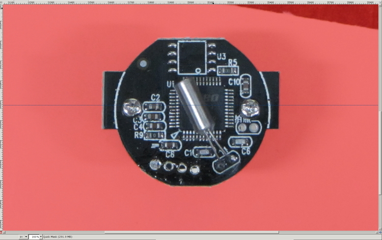
    Use the Magic Scissors to select the PCB border (it’s the nearly invisible ragged dotted outline):

    Camera PCB - scissors selection - scaled
    Camera PCB – scissors selection – scaled

    Flip to Quick Mask mode and clean up the selection as needed:

    Camera PCB - quick mask cleanup - scaled
    Camera PCB – quick mask cleanup – scaled

    Flip back to normal view, invert the selection (to select the background, not the PCB), and delete the background to isolate the PCB:

    Camera PCB - isolated - scaled
    Camera PCB – isolated – scaled

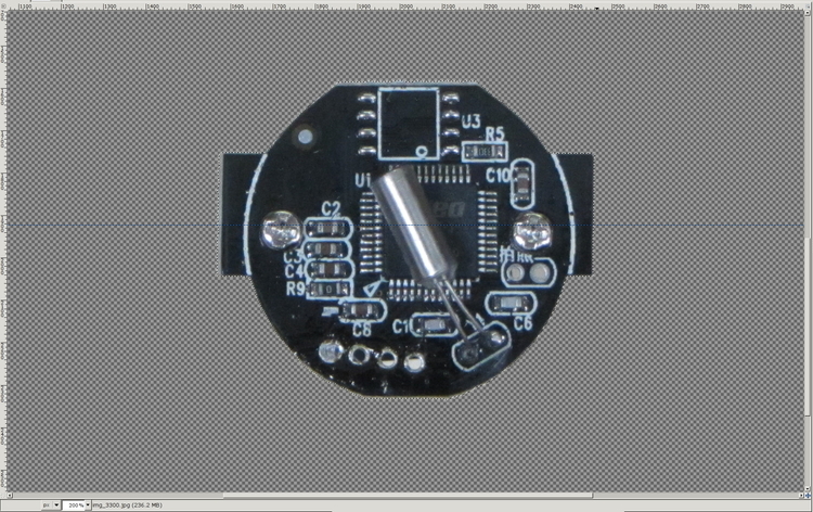
    Tight-crop the PCB and flatten the image to get a white background:

    Camera PCB - isolated - scaled
    Camera PCB – isolated – scaled

    Fetch some digital graph paper from your favorite online source. The Multi-color (Light Blue / Light Blue / Light Grey) Multi-weight (1.0×0.6×0.3 pt) grid (1 / 2 / 10) works best for me, but do what you like. Get a full Letter / A4 size sheet, because it’ll come in handy for other projects.

    Open it up (converting at 300 dpi), turn it into a layer atop the PCB image, use the color-select tool to select the white background between the grid lines, then delete the selection to leave just the grid with transparency:

    Camera PCB with grid overlay - unscaled
    Camera PCB with grid overlay – unscaled

    We want one minor grid square to be 1×1 mm on the PCB image, sooo…

    • Accurately measure a large feature on the real physical object: 27.2 mm across the tabs
    • Drag the grid to align a major line with one edge of the PCB
    • Count the number of minor square across to the other side of the image: 29.5
    • Scale the grid overlay layer by image/physical size: 1.085 = 29.5/27.2
    • Drag the grid so it’s neatly centered on the object (or has a major grid intersection somewhere useful)

    That produces a calibrated overlay:

    Camera PCB with grid overlay
    Camera PCB with grid overlay

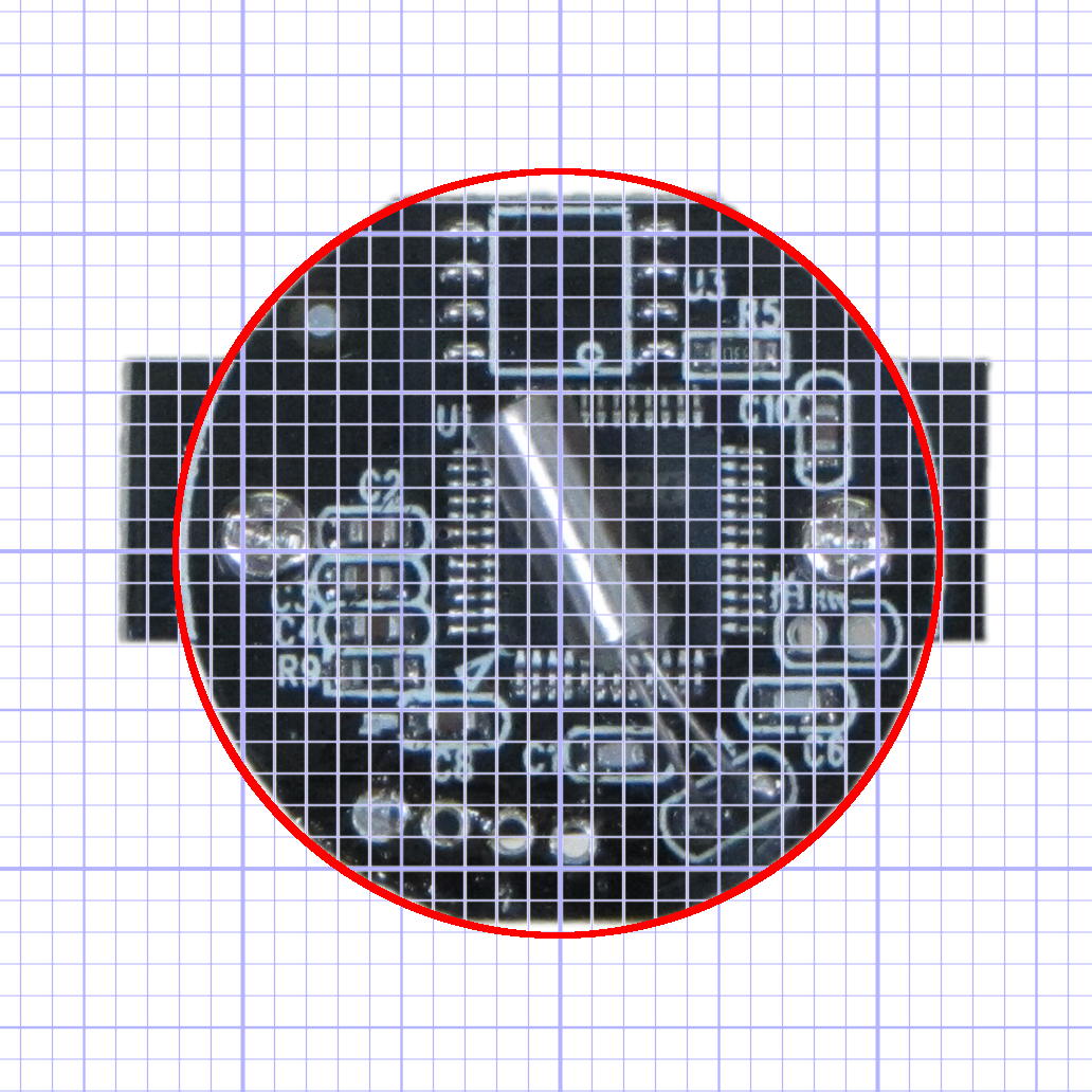
    Then it’s just a matter of reading off the coordinates, with each minor grid square representing 1.0 mm in the real world, and writing some OpenSCAD code…

  • Jerusalem Cricket vs. Dust Bunny

    Sometimes crickets make their way into the basement. This one, a model that I’ve always known as a Jerusalem Cricket(*) evidently lost a pitched battle with one of the Dust Bunnies guarding the Basement Laboratory:

    Jerusalem Cricket vs Dust Bunny - top view
    Jerusalem Cricket vs Dust Bunny – top view

    A rear view:

    Jerusalem Cricket vs Dust Bunny - rear view
    Jerusalem Cricket vs Dust Bunny – rear view

    From the front:

    Jerusalem Cricket vs Dust Bunny - front view
    Jerusalem Cricket vs Dust Bunny – front view

    I deported it to the flower garden outside the basement door, where I hope it can brush off the Bunny’s entrapments…

    It may not be a Jerusalem Cricket, because they’re more common out west, but that’s the best match in our bug books and that’s what we’ve always called them.

    [Update: (*) It’s most likely a Cave Cricket. See the comments for details.]

  • Too Many Deer: Aftermath

    We spotted this crumpled front end at a local repair shop:

    Deer crash damage - overview
    Deer crash damage – overview

    A closer look at the bumper tells the tale:

    Deer crash damage - hair detail
    Deer crash damage – hair detail

    Pop Quiz: estimate the total cost of that collision, including the overhead of having to deal with the insurance company and arrange alternate transportation for a week or two.

    Essay: explain why it’s possible for someone to insist that both deer and humans are better off under these conditions.

    In this area, vehicles serve as the top predator for deer…

  • SMD-to-DIP Adapter: Pin Soldering “Fixture”

    I needed a rail-to-rail op amp in a DIP package to breadboard the amplifier for those toroids and came up dry, so I sawed out a protoboard square, glued a MAX4330 in SOT23-5 atop it in classic dead-bug style, rearranged the leads into the standard DIP pinout, and moved on:

    MAX4330 dead-bug style on DIP adapter
    MAX4330 dead-bug style on DIP adapter

    The trick to getting the header pins aligned is to stick ’em in a pile of perfboards, which instantly makes them stand up straight and parallel:

    img_3430 - SMD-to-DIP adapter - PCB soldering fixture
    img_3430 – SMD-to-DIP adapter – PCB soldering fixture

    Stick the square adapter atop the headers, solder all eight pins, glue down the SOT23, and solder it with wire-wrap snippets. Ugly, but workable…

  • Air-gapped Ferrite Toroid Data

    For an upcoming Circuit Cellar column on Hall effect current sensing, I slit another pair of toroids:

    Slitting FT37 ferrite toroid
    Slitting FT37 ferrite toroid

    Then wound them with grossly excessive amounts of wire (the up-armored core on the right appeared earlier):

    Slit Ferrite Toroid current sensors
    Slit Ferrite Toroid current sensors

    The smaller toroid is an FT37-43 that barely covers the active area of an SS49-style Hall effect sensor, but experience with the FT50 toroid suggests that’ll be entirely enough:

    slit FT37 toroid trial fit to SS48-style Hall effect sensor
    slit FT37 toroid trial fit to SS48-style Hall effect sensor

    Data on the uncut toroids:

    Property FT50-61 FT37-43
    Outer diameter (OD) – inch 0.50 0.375
    Inner diameter (ID) – inch 0.281 0.187
    Length – inch 0.188 0.125
    Cross section area – cm2 0.133 0.133
    Mean path length (MPL) – cm 3.02 2.15
    Volume – cm3 0.401 0.163
    Relative Permeability (μr ) 125 850
    Saturation flux G @ 10 Oe 2350 2750
    Inductance factor (AL) – nH/turn2 68.0 420

    Those overstuffed windings improved the sensitivity, but increased the winding resistance far beyond what’s reasonable.

    Data on the slit toroids:

    Toroid ID FT50-61 FT37-43 FT50-61
    Measured air gap – cm 0.15 0.15 0.17
    Winding data
    Turns 120 80 25
    Wire gauge – AWG 28 32 26
    Winding resistance – mΩ 530 920 100
    Predicted B field – G/A 872 660 163
    Hall effect sensor @ 1.9 mV/G
    Predicted output – mV/mA 1.7 1.3 0.31
    Actual output – mV/mA 1.9 1.9 0.37
    Actual/predicted ratio – % +12 +46 +19

    The last few lines in that table show the transimpedance (transresistance, really, but …) based on the winding current to Hall sensor output voltage ratio (in either mV/mA or V/A, both dimensionally equivalent to ohms), which is why the toroid’s internal magnetic flux doesn’t matter as long as it’s well below saturation.

    Gnawing the 80 turn winding off the FT37-43 toroid and rewinding it with 15 turns of 24 AWG wire dropped the winding resistance to 23 mΩ and the transimpedance to 0.36 mV/mA:

    FT37-43 with 15 turns 24 AWG - Hall sensor
    FT37-43 with 15 turns 24 AWG – Hall sensor

    However, applying a voltage gain of about 28 (after removing the sensor’s VCC/2 bias) will produce a 0-to-5 V output from 500 mA input, which seems reasonable.

  • Wouxun KG-UV3D Batteries: Age and Cycle Effects

    The first Wouxun (evidently pronounced “ocean”) KG-UV3D HT spent a month or two in my bike, lashed to a kludged version of the APRS+voice interface box and powered by its own lithium-ion pack. After I got the circuit worked out and built a duplicate, I picked up a second HT for Mary’s bike; as a result, that battery pack never got much use.

    A pair of discharge tests shows the difference:

    Wouxun 7.4 V Packs
    Wouxun 7.4 V Packs

    The 2011-03 battery has almost exactly the rated 1.7 A·h capacity, at least if you’re willing to run it down to 6 V, and the 2012-06 pack delivers 1.9 A·h. Electronic gadgets measure state-of-charge using the battery voltage, so the older pack “looks” like it has much less capacity: it runs about 100 mV lower than the newer pack out to 1.2 A·h, then falls off the cliff. Looks to me like one of the two cells inside is fading faster than the other; so it goes.

    I’m still thinking of using these to power some LED taillights, because they have a nice form factor and built-in latches:

    Wouxun KG-UV3D - battery pack latch
    Wouxun KG-UV3D – battery pack latch
  • Blueberry Season: Stink Bug Eggs

    Mary’s been picking blueberries and freezing them for winter treats, a process that involves inspecting each berry laid out on the tray.

    This one failed QC:

    Blueberry with eggs - overview
    Blueberry with eggs – overview

    A closer look shows some remarkable structures:

    Blueberry with eggs - detail
    Blueberry with eggs – detail

    Unfortunately, they’ll probably turn into Brown Marmorated Stink Bugs. This is not a Good Thing, because those stink bugs will devastate fruit harvests, including all the apple orchards along the entire Hudson Valley, over the next few years.

    They may be Predatory Stink Bugs, which would be unusual in Dutchess County, but not nearly so awful.