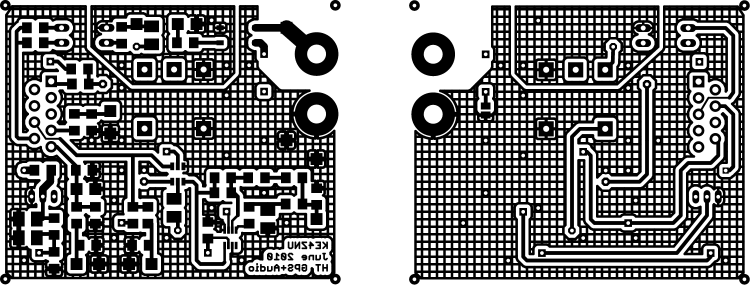
The circuit board is 30-mil, double-sided, half-ounce (I think) copper on glass-fiber stock, direct-etched by rubbing ferric chloride solution onto it with a sponge.
Used the CNC Sherline to drill the holes; the G-Code is now tailored for my Sherline mill and tool-length probe station.
The copper layers as a 600 dpi PNG file:

The top copper image (on the left) is reversed so it comes out correctly when you’re doing toner-transfer etching.
I didn’t bother with a silkscreen, because I don’t have a soldermask and there’s no room for text around the parts anyway.
The four vias at the corners mark the edge of the board. Trim it with tinsnips (or a shear if you have one), then introduce it to Mr Belt Sander until the edges pass directly through the middle of those via holes. Round the corners a bit so they fit into the case recess atop the mounting shoulder.
Put Z-wires in the small round vias (the ones that don’t have any other traces) to connect the top and bottom ground planes.
Put Z-wires in the other round vias to connect a top-side signal to the corresponding bottom-side trace.
There are three jumper wires across the bottom; with only two layers I don’t get all bothered about embedding the last few. Those vias are square.
I don’t have any way to do plated-through holes, so solder the wires to both sides of any vias with traces on both planes. I admit I missed two of them on the TT3 ribbon cable.
The big empty space around the positive power terminal prevents the ring-lug connector from shorting to the ground plane. Now that I think of it, there’s no need for an empty space on the bottom copper, but it doesn’t do any harm.
Comments
4 responses to “HT GPS + Audio: PCB Layout”
My circuit board plotter doesn’t do through-hole vias so I spend a lot of time soldering in wires from side to side. What I’ve found works better for me than z-wires is a long bus wire that I thread through all the holes on the entire board, solder on both sides, then clip. The reason that seems to work better is that it’s hard for me to get the bends that prevent the wire falling through, aligned with the traces rather than shorting to adjacent material.
thread through all the holes on the entire board
Now that’s a good idea!
I start with a generous length of wire, stick each end through a hole, bend them over with the butt end of the tweezers, and solder in place. Snip the other side, bend, and solder. Repeat until I can’t find any more holes. Take a break, return, and finish the last half-dozen holes …
The loop between the holes keeps the wire aligned, so the bend on the other side stays roughly where you put it. It’s not possible, alas, to hold the loop with my fingers while soldering, though, no matter how often I try.
When I’m in pennypinching mode I save the butt ends of LED leads and such, and do the same, but that lacks the ‘generous length’ bit. However, at work, because of a communications breakdown, we just got about 300,000 feet of wire that someone ordered in error, including rather a lot of bus wire, so I don’t think I’ll be reusing cut-off leads for quite a while.
Some of the snippets in my little tin of component cutoffs have probably been in there for two decades… but ya can’t just throw ’em out!
300,000 feet of wire that someone ordered in error
A friend of mine bungled the “unit of measure” on an order and wound up with a semitrailer load of exotic photosensitive copier paper that required a controlled storage environment. For years thereafter, every raised floor in the IBM site had a few cartons of the stuff…