Ed Nisley's Blog: Shop notes, electronics, firmware, machinery, 3D printing, laser cuttery, and curiosities. Contents: 100% human thinking, 0% AI slop.
Running some serial I/O in the background adds jitter to the timer interrupt pacing the ADC samples and as-yet-unwired DDS updates. For reference, an overview of the process showing the procession from the IRQ on the left to the SPI outputs near the middle and another IRQ on the far right:
DDS Mock – 0 VAC – SPI
Now, speed up the sweep and delay the trace by 25 μs to put the triggering pulse off-screen to the left and the second pulse at the center division:
ADC Sample IRQ jitter
The orange smear in the middle should be a tidy pulse, but it isn’t.
The 25 μs timer interrupt now has the highest priority on the front burner:
IntervalTimer AudioSampler;

... snippage ...

  AudioSampler.priority(0);
  if (!AudioSampler.begin(AudioSamplerIRQ, SamplePeriod)) {
    Serial.printf("Timer start failed\n");
    while (true) {
      FlipPin(BUILTIN_LED);
      delay(75);
    }
  }
Although nothing can interrupt it, other code / handlers may disable interrupts around their own critical sections and delay the tick. If the triggering tick (the off-screen one starting the trace) is delayed, then the on-screen pulse will appear “too soon”, to the left of center. If the triggering tick is on time, but the on-screen pulse is delayed, it’ll appear “too late” on the right.
The blur is (roughly) symmetric around the center graticule line, so the handwaving seems about right.
In round numbers, the jitter moves the interrupt ±325 ns on either side of its nominal position, with most of the pulses within ±100 ns. I doubt the jitter distribution is Gaussian, but vigorous handwaving says the RMS jitter might amount to 75 ns.
At the 4 kHz audio band limit, a 75 ns sampling error a phase error of 0.1°, so the maximum amplitude jitter would be sin(0.1°) = 0.002 = -55 dB, which might suffice for amateur-radio audio.
Doing the DDS calculations in full-frontal double floating point turns out to be maybe fast enough:
DDS Mock – 0 VAC – SPI
I set the ADC to HIGH_SPEED conversion and sampling, reducing the time between the start of conversion (first pulse in D1) and the ADC end-of-conversion interrupt (rising edge in D2) from 4.7 μs to 2.6 μs, more-or-less, kinda-sorta.
The ADC hardware can return the average of several sample taken in quick succession, so I set it to average four samples. The vertical cursors show the combination of fast conversion and averaging requires 7 μs (-ish) from start to finish: long enough to justify separating the two by an interrupt and short enough to allow calculations after fetching the result.
The purple trace shows the analog input voltage hovering close to a constant VCC/2 (about 1.6+ V), rather than the sine-wave I used earlier, again courtesy of the scope’s arbitrary function generator. The loop() dumps the min and max ADC values (minus half the ADC range (4096/2= 2048):
    -4 to     2
    -3 to     2
    -3 to     2
A span of half a dozen counts = 3 bits means the 12 bit ADC really delivers 9 bits = 0.2% resolution = 54 dB dynamic range = probably not good enough. However, the “circuit” is an open-air hairball on the bench, driven from the scope’s arbitrary waveform generator in high-Z mode, so things can only get better with more any attention to detail.
The 1.9 μs gap between the first and second burst of SPI clocks contains all the floating-point calculations required to convert an ADC sample to DDS delta-phase bits:
void adc0_isr(void) {

  int Audio;

  digitalWriteFast(PIN_ANALOG,HIGH);

  AnalogSample = adc->readSingle();             	  // fetch just-finished sample
  Audio = AnalogSample - 2048;                      // convert to AC signal

  DDSBuffer.Phase = 0;

  SPI.beginTransaction(SPISettings(8000000, MSBFIRST, SPI_MODE0));
  digitalWriteFast(PIN_DDS_FQUD, LOW);

  SPI.transfer(DDSBuffer.Phase);

  DDSBuffer.DeltaPhase = (uint32_t)((((double)Audio / 2048.0) * Deviation + Crystal) * CountPerHertz);

  SPI.transfer((uint8_t)(DDSBuffer.DeltaPhase >> 24));      // MSB first!

  if (Audio > AudioMax)                                     // ignore race conditions
    AudioMax = Audio;
  if (Audio < AudioMin) AudioMin = Audio; SPI.transfer((uint8_t)(DDSBuffer.DeltaPhase >> 16));

  SPI.transfer((uint8_t)(DDSBuffer.DeltaPhase >>  8));
  SPI.transfer((uint8_t)DDSBuffer.DeltaPhase);

  SPI.endTransaction();                         // do not raise FQ_UD until next timer tick!

  digitalWriteFast(PIN_ANALOG,LOW);
}
A closer look lets the scope decode and present the SPI data:
DDS Mock – 0 VAC – SPI detail
The program calculates and displays various “constants” I set for convenience:
FM Modulated DDS
Ed Nisley KE4ZNU
 serial wait: 890 ms

DDS clock:     180000000.000 Hz
CountPerHertz:        23.861 ct
HertzPerCount:         0.042 Hz

Crystal:    20000000.000 Hz
Deviation:      5000.000 Hz
You can confirm the SPI data by working backwards with a calculator:
This file contains hidden or bidirectional Unicode text that may be interpreted or compiled differently than what appears below. To review, open the file in an editor that reveals hidden Unicode characters.
Learn more about bidirectional Unicode characters
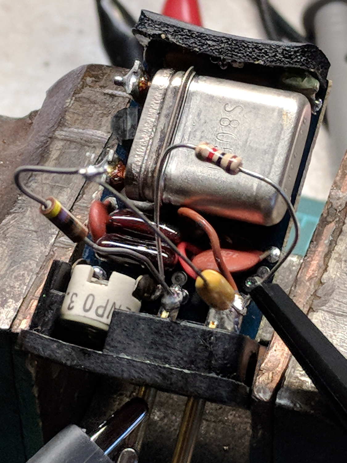
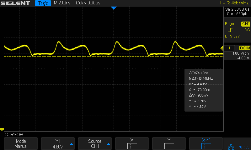
For lack of anything smarter, I put a 1 kΩ resistor from RF Out to Ground to get some DC current going, then used a 470 nF cap and 47 Ω resistor as an AC load:
K1003 Channel Element – bias lashup
Which oscillated around a mid-scale DC bias, but looked ugly:
K1003 Channel Element – 13.4 MHz output – 1k bias
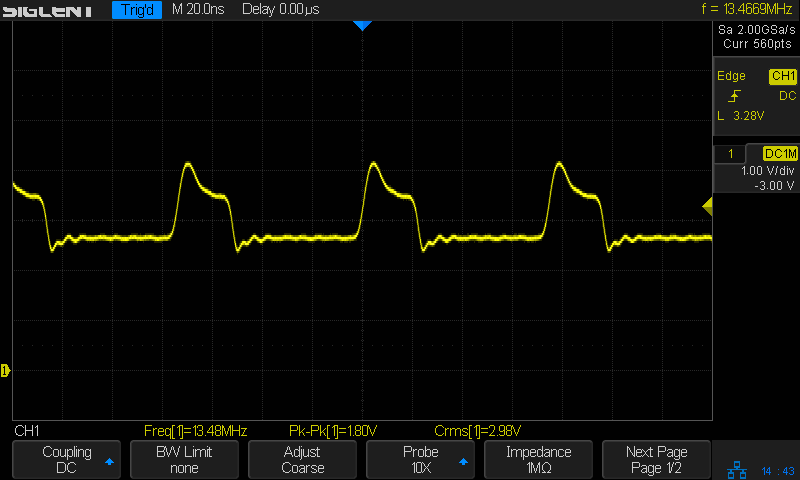
Perusing some receiver schematics suggested a heavier DC load, so I swapped in a 470 Ω resistor:
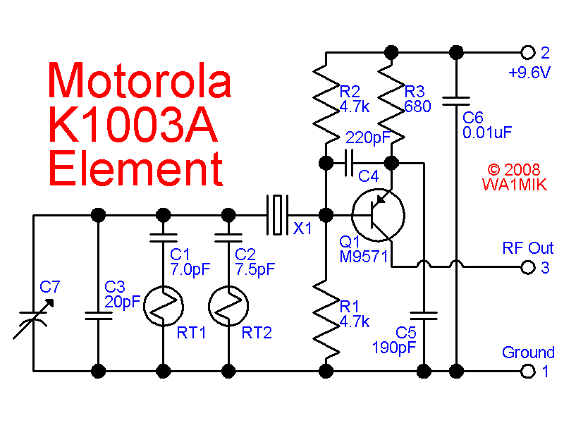
The general idea is to frequency modulate the sine wave coming from a DDS, thereby generating a signal suitable for upconverting in amateur repeaters now tied to unobtainable crystals. The crystals run from 4-ish to 20-ish MHz, with frequency multiplication from 3 to 36 producing RF outputs from 30-ish MHz through 900-ish MHz; more details as I work through the choices.
The demo code runs on a bare Teensy 3.6 as a dipstick test for the overall timing and functionality:
FM DDS – Teensy 3.6 SPI demo
The fugliest thing you’ve seen in a while, eh?
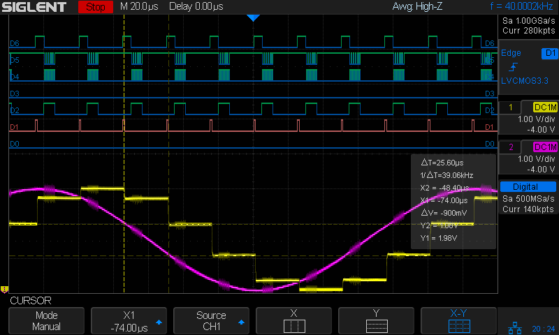
An overview of the results:
Analog 4 kHz @ 40 kHz – SPI demo overview
The pulses in D1 (orange digital) mark timer ticks at a 40 kHz pace, grossly oversampling the 4 kHz audio bandwidth in the hope of trivializing the antialiasing filters. The timer tick raises the DDS latch pin (D6, top trace) to change the DDS frequency, fires off another ADC conversion, and (for now) copies the previous ADC value to the DAC output:
The purple analog trace is the input sine wave at 4 kHz. The yellow analog stairstep comes from the DAC, with no hint of a reconstruction filter knocking off the sharp edges.
The X1 cursor (bold vertical dots) marks the start of the ADC read. I hope triggering it from the timer tick eliminates most of the jitter.
The Y1 cursor (upper dotted line, intersecting X1 just left of the purple curve) shows the ADC sample apparently happens just slightly after the conversion. The analog scales may be slightly off, so I wouldn’t leap to any conclusions.
The pulses in D2 mark the ADC end-of-conversion interrupts:
void adc0_isr(void) {
  digitalWriteFast(ANALOG_PIN,HIGH);
  AnalogSample = adc->readSingle();                     // fetch just-finished sample
  SPI.beginTransaction(SPISettings(8000000, MSBFIRST, SPI_MODE0));
  digitalWriteFast(DDS_FQUD_PIN, LOW);
  SPI.transfer(DDSBuffer.Phase);                // interleave with FM calculations
  SPI.transfer(DDSBuffer.Bits31_24);
  SPI.transfer(DDSBuffer.Bits23_16);
  SPI.transfer(DDSBuffer.Bits15_8);
  SPI.transfer(DDSBuffer.Bits7_0);
  SPI.endTransaction();                         // do not raise FQ_UD until next timer tick!
  digitalWriteFast(ANALOG_PIN,LOW);
}
The real FM code will multiply the ADC reading by the amplitude-to-frequency-deviation factor, add it to the nominal “crystal” frequency, convert the sum to the DDS delta-phase register value, then send it to the DDS through the SPI port. For now, I just send five constant bytes to get an idea of the minimum timing with the SPI clock ticking along at 8 MHz.
The tidy blurs in D4 show the SPI clock, with the corresponding data in D5.
D6 (top trace) shows the DDS FQ_UD (pronounced “frequency update”) signal dropping just before the SPI data transfer begins. Basically, FQ_UD is the DDS Latch Clock: low during the delta-phase value transfer, with the low-to-high transition latching all 40 control + data bits into the DDS to trigger the new frequency.
A closer look at the sample and transfer:
Analog 4 kHz @ 40 kHz – SPI demo detail
For reference, the digital players from bottom to top:
D0 – unused here, shows pulses marking main loop
D1 – 40 kHz timer ticks = ADC start conversion
D2 – ADC end of conversion,”FM calculation”, send DDS data
D3 – unused here, shows error conditions
D4 – SPI clock = rising edge active
D5 – SPI MOSI data to DDS = MSB first
D6 – SPI CS = FQ_UD = DDS latch
Remember, the yellow analog stairstepped trace is just a comfort signal showing the ADC actually samples the intended input.
Dropping the sampling to 20 kHz would likely work just as well and double the time available for calculations. At least now I can measure what’s going on.
All in all, it looks feasible.
And, yes, the scope is a shiny new Siglent SDS2304X with the MSO logic-analyzer option. It has some grievous UX warts & omissions suggesting an architectural botch job, but it’s mostly Good Enough for what I need. More later.
This file contains hidden or bidirectional Unicode text that may be interpreted or compiled differently than what appears below. To review, open the file in an editor that reveals hidden Unicode characters.
Learn more about bidirectional Unicode characters
The objective is to capture screen shots from the HP 8591 spectrum analyzer, now connected to Serial Port 2 of the Sena PS410 serial server.
My analyzer is an old one with a 3322A serial number, so its Opt 023 came with a genuine DB-25 female connector, not the DE-9 male connector described in the HP doc for the later Op 043 hardware. With that in mind, the HP doc says the spectrum analyzer supports only hardware handshaking:
Baud rate 300 to 57,000 baud.
8 bits per character.
1 stop bit.
No parity.
Software handshake – none.
Xon/Xoff and ENQ/ACK not supported by the spectrum analyzer.
The manual enumerates the handshaking lines:
Request to send (RTS) – Output signal indicates that the spectrum analyzer is ready to communicate. This line is true at power-up and stays true while power is on.
Clear to send (CTS) – Input signal indicates that the external controller is ready to receive data.
Data terminal ready (DTR) – Output signal from the spectrum analyzer. When the input buffer is full, this line goes false.
Data set ready (DSR) – Is not available.
Data carrier detect (DCD) – Input to the spectrum analyzer. If DCD is true, the spectrum analyzer will receive data from the controller. If false, no data will be input. The data will be ignored.
Furthermore, it is written:
The spectrum analyzer checks its CTS input before transmitting data to the computer. If the CTS line is false, the spectrum analyzer will not transmit data. The spectrum analyzer transmits data when the CTS line is true.
The spectrum analyzer sets the DTR line (PC CTS) false when its input buffer is full.
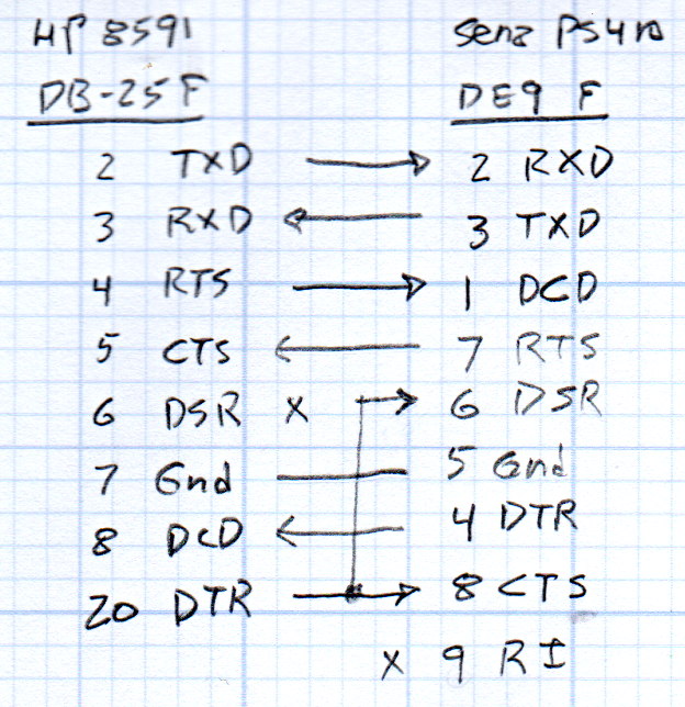
They offer several wiring diagrams, none of which correspond to the hardware on my bench, but swapping the “Personal Computer” and “Analyzer” headings on this diagram seems close to reality:
HP 8591 – RS232 DB25 to DE9 wiring diagram
On the other end of the cable, the PS410 does “hardware flow control using RTS/CTS”. They also offer a diagram:
Sena PS410 – RS232 wiring diagram
So I rewired the cable thusly:
HP 8591 vs Sena PS410 – RS232 cable diagram
Pin 1 on the 8591 interface connects to both frame ground and signal ground and, back when I first made this cable, many years ago, I had wired it to the shield of the cable and thence to the DE9 shell. Alas, the PS410 took offense; for reasons I don’t understand, a shell-to-ground connection ignites a ferrite bead on the PS410’s PCB.
With the rewired cable in hand, the PS410 serial port setup looks like this:
Port 2 – 8591 serial config
The PS410 apparently wiggles its RTS output after every byte it receives, because the CTS input at the 8591 turns into a blur during screen captures. This seems unaffected by the Inter character time-out setting and doesn’t (seem to) produce any problems, so it’s like that and that’s the way it is.
Using 9600 b/s isn’t as slow as you might think. The HP manual notes:
Some of the programs in this manual use 1200 baud for proper operation. If your system uses the RS-232 handshake lines, you can use 9600 baud for all of the programs.
I tried 19200 b/s and got mysterious errors that resemble overruns, which suggests the 8591 ignores the PS410’s flickering RTS output. The screen dumps require only a few seconds, so it’s not a big deal, although timing issues have a way of resurfacing at the most inopportune, uh, times.
Kermit knows how to handle network sockets and suchlike, so aiming it at the spectrum analyzer is a one-liner:
set host 192.168.1.40 7002 /raw-socket
set modem none
The /raw-socket disables Kermit’s default Telnet interface, preventing it from squirting IAC + BRK characters when closing the session; I think that’s what happens, but I don’t use Telnet enough to know better. As you might expect, the 8591 deals poorly with characters outside its lexicon.
It’s not obvious set modem none does anything in this context, but it seems reasonable.
Then the rest of the script Just Works:
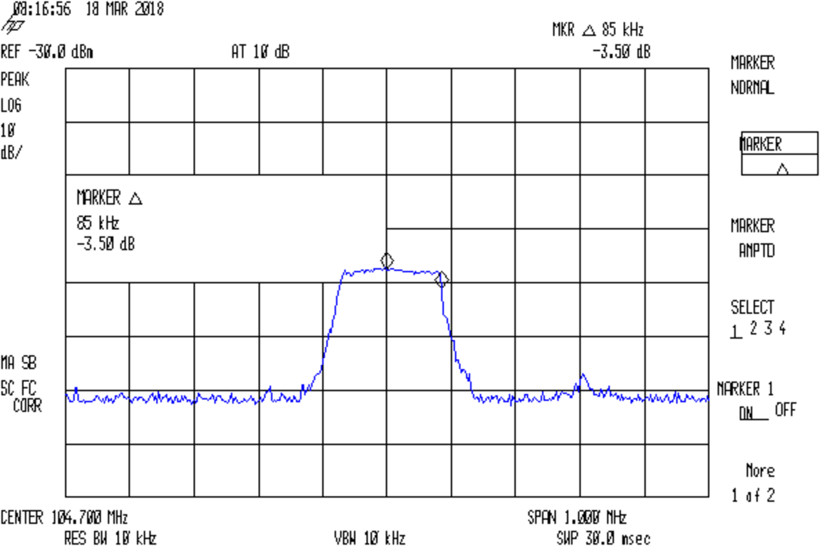
FM 104.7 MHz peak hold
Which is the peak-hold spectrum of a local FM station, as received through an amateur radio HT rubber duck antenna.
This file contains hidden or bidirectional Unicode text that may be interpreted or compiled differently than what appears below. To review, open the file in an editor that reveals hidden Unicode characters.
Learn more about bidirectional Unicode characters