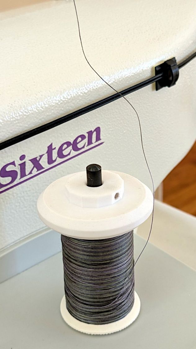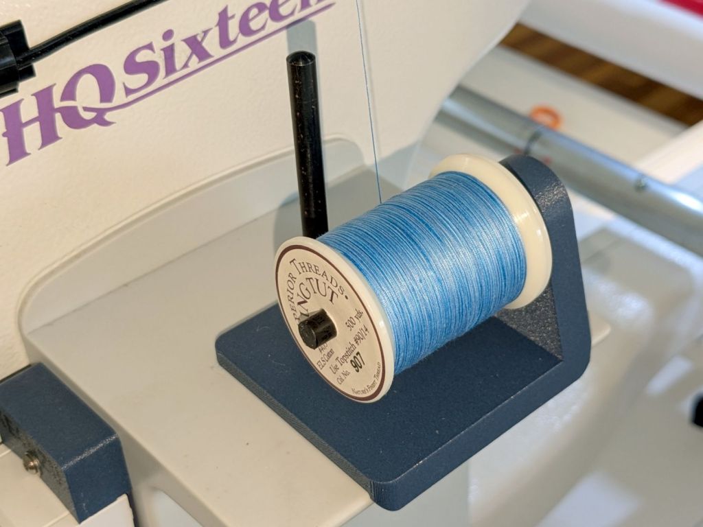
After watching the thread pull off the spool around the vertical spool adapter in an increasingly tight helix, I built a horizontal adapter:

The thread now pulls off perpendicular to the axis, the way we thought it should, and the helix is gone.
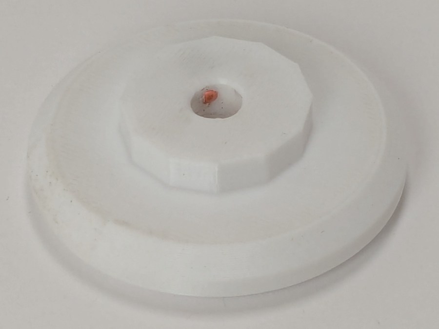
The adapter base plate fits snugly over the vertical pin, with the lip over the edge stabilizing the whole thing. The spool fits on a ¼ inch acrylic rod tightly press-fit into the side wall and, although it’s not shown here, the vertical adapter press-fits onto the end of the rod to keep the spool from wandering off.
The solid model shows the arrangement:

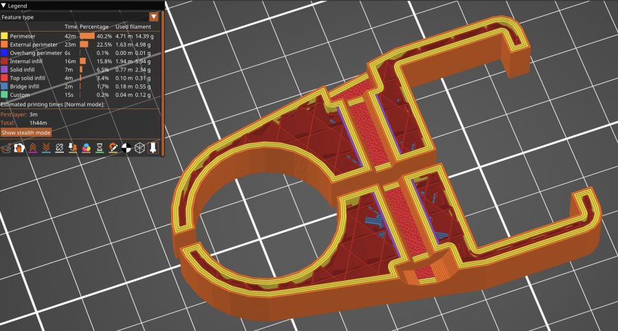
It builds standing on the wall to prevent any significant overhang:

So we’ve reconfirmed our original knowledge that ordinary thread spools must feed off the side, not over the top. Living in the future with rapid prototyping and simple production is good!
You can buy a Horizontal Spool Pin Clamp, but what’s the fun in that?
Fun fact: although the vertical pins on the machine are ¼ inch in diameter, the thread on the end is neither the obvious ¼-20 nor the second-guess 10-32. Instead, it’s M5×0.8, perilously close to the 10-32 thread used in the handlebar setscrews. Don’t apply brute force when this thing doesn’t screw neatly into that hole.
The OpenSCAD source code as a GitHub Gist:
| // HQ Sixteen – horizontal thread spool adapter | |
| // Ed Nisley – KE4ZNU | |
| // 2025-01-26 | |
| include <BOSL2/std.scad> | |
| Layout = "Show"; // [Show,Build,Base,Wall] | |
| /* [Hidden] */ | |
| ID = 0; | |
| OD = 1; | |
| LENGTH = 2; | |
| WallThick = 10.0; | |
| BaseThick = 5.0; | |
| PinOD = 0.25*INCH; // vertical spool pin | |
| PinWasher = [PinOD,11.0,2.0]; // pin base washer | |
| PinOffset = 49.0; // pin center to edge of platform | |
| Spool = [0.25*INCH,50.0,55.0]; // maximum thread spool | |
| echo(Spool=Spool); | |
| SpoolClearance = [5.0,2.0,5.0]; | |
| SpoolOC = [-PinOffset + PinOD/2 + SpoolClearance.x + Spool[OD]/2, | |
| Spool[LENGTH]/2, | |
| BaseThick + SpoolClearance.z + Spool[OD]/2]; | |
| BasePlate = [PinWasher[OD] + PinOffset + BaseThick, | |
| Spool[LENGTH] + SpoolClearance.y + WallThick, | |
| BaseThick]; | |
| Protrusion = 0.1; | |
| $fn = 12*3*4; // smooth outer perimeters | |
| //———- | |
| // Construct the pieces | |
| module Base() { | |
| difference() { | |
| union() { | |
| left(BasePlate.x/2 – BaseThick) back((SpoolClearance.y + WallThick)/2) | |
| cuboid(BasePlate,rounding=BaseThick,edges=[FWD+LEFT,FWD+RIGHT],anchor=BOTTOM); | |
| back((SpoolClearance.y + WallThick)/2) | |
| cuboid([BaseThick,BasePlate.y,BaseThick], | |
| rounding=BaseThick,edges=[FWD+BOTTOM,FWD+RIGHT,BACK+BOTTOM],anchor=LEFT+TOP); | |
| } | |
| left(PinOffset) down(Protrusion) { | |
| cylinder(PinWasher[LENGTH],d=PinWasher[OD]); // washer clearance | |
| cylinder(2*BaseThick,d=PinOD); | |
| } | |
| } | |
| } | |
| module Wall() { | |
| difference() { | |
| union() { | |
| hull() { | |
| right(BaseThick) | |
| cube([BasePlate.x,BaseThick,WallThick],anchor=FWD+RIGHT+BOTTOM); | |
| back(SpoolOC.z) right(SpoolOC.x) | |
| cylinder(d=Spool[OD]/2,h=WallThick); | |
| } | |
| back(SpoolOC.z) right(SpoolOC.x) | |
| cylinder(d=Spool[OD]/2,h=WallThick + SpoolClearance.y); | |
| } | |
| back(SpoolOC.z) right(SpoolOC.x) down(Protrusion) zrot(180/8) | |
| cylinder(d=Spool[ID],h=2*WallThick,$fn=8); | |
| } | |
| } | |
| module Adapter() { | |
| union() { | |
| Base(); | |
| back(SpoolOC.y + SpoolClearance.y + WallThick) | |
| xrot(90) | |
| Wall(); | |
| } | |
| } | |
| //———- | |
| // Show & build the results | |
| if (Layout == "Base") | |
| Base(); | |
| if (Layout == "Wall") | |
| Wall(); | |
| if (Layout == "Show") { | |
| Adapter(); | |
| left(PinOffset) | |
| color("Gray") { | |
| cylinder(d=PinOD,h=2*SpoolOC.z); | |
| cylinder(d=PinWasher[OD],h=PinWasher[LENGTH]); | |
| } | |
| up(SpoolOC.z) right(SpoolOC.x) back(SpoolOC.y) | |
| xrot(90) | |
| color("Green") | |
| cylinder(d=Spool[ID],h=Spool[LENGTH]); | |
| } | |
| if (Layout == "Build") | |
| up(SpoolOC.y + SpoolClearance.y + WallThick) | |
| xrot(-90) | |
| Adapter(); | |