Ed Nisley's Blog: Shop notes, electronics, firmware, machinery, 3D printing, laser cuttery, and curiosities. Contents: 100% human thinking, 0% AI slop.
Without much tuning at all the Peltier module holds the MOSFET-under-test block within the ±1 °C deadband for heating to 30 °C:
Bringup Test – Igain 0.01
And it’s pretty close for cooling to 10 °C:
Bringup Test – Cool – Igain 0.01
The PWM and Integral traces refer to the right-hand Y axis scale, the rest to the left. The total elapsed time is a bit under 3 minutes, but it’s measured in samples because I’m not going to bother with a formal timebase for this thing.
The Basement Laboratory is around 14 °C right now, so cooling isn’t all that much of a problem.
The code doesn’t really run a PI loop: it switches from P control outside the deadband to I control inside, preloading the integral accumulator to maintain the PWM value at the inbound switchover. That sidesteps the whole integral windup problem, which seems like a Good Idea, but a quick test at 50 °C says the P control may not have enough moxie to reach the deadband and the I control seems overenthusiastic.
More fiddling is definitely in order.
So far, the machinery looks like this:
rDS Tester – Peltier Tests
The aluminum block toward the rear holds the MOSFET and the thermistor atop the Peltier module, all stuck on the black CPU cooler with the fan on the bottom. The various heatsinks are obviously scrounged from the heap and are much too large; some fine tuning is in order now that the temperature’s nailed down.
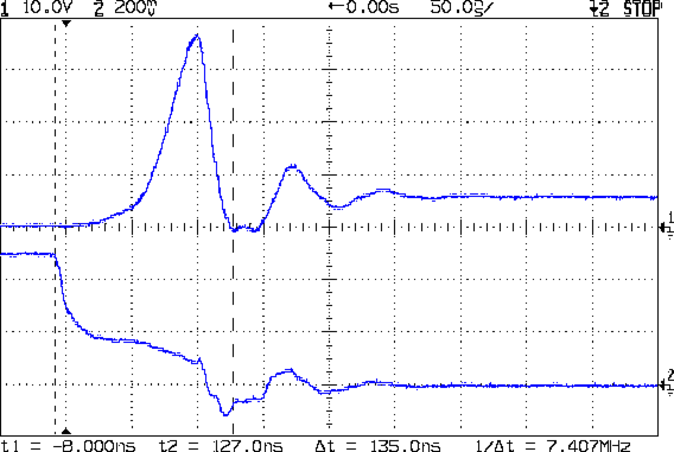
On the other end of the Peltier driver’s PWM pulse, the MOSFET turns on with a surprisingly lengthy time constant:
Peltier Drain – Turn-On
The upper trace shows the drain voltage drops to nearly 0 V as the transistor turns on, then rises to about 600 mV. The IRLZ14 spec says RDS is 200 mΩ max, so that’s in line with the actual 3.3 A through the Peltier module, and puts the dissipation at 2.2 W.
The lower trace is the gate drive, showing a small Miller effect. The Channel 2 scale readout is off by a factor of 10, as I forgot to tell the scope that I was using a 10x probe. It’s really 5 V/div, not 500 mV/div.
The cursors put the time constant at 1.3 µs. If the inductance is the 5.4 µH indicated by the turn-off resonance, then the total circuit resistance is nearly 4 Ω… which is obviously not the case, given the 5 V supply voltage and the 3.3 A current.
Looking at the Peltier module’s power supply at the board terminal reveals the true cause:
Peltier Supply Transient
The scale is 1 V/div with 0 V at the bottom of the screen , so the switching supply produces 5.2 V with no load and 4.6 V at about 3 A. It’s rated at 5 V and 3.7 A, so the Peltier current is right up near its limit.
The glitch when the MOSFET turns off shows that the supply can’t absorb much transient power in either direction, which is typical of switching supplies. In this day & age, there’s no bulk capacitance to smooth out line-frequency ripples from a full-bridge rectifier.
The total circuit resistance is about 1.8 Ω, figuring the Peltier module at 1.5 Ω, the MOSFET at 0.2 Ω, and everything else at 0.1 Ω. That says the actual current is around 2.6 A, although the fancy Tek Hall Effect probe I mooched from Eks puts it at almost exactly 3 A; I’d tend to trust the Tek probe’s opinion more than my sum of small numbers. With 4.6 V and 3 A, the total resistance is spot on 1.5 Ω. The Peltier module’s resistance is temperature sensitive, so a few tenths of an ohm variation isn’t entirely unexpected.
So that says the L/R time constant is (5.4 µH / 1.5 Ω) = 3.6 µs, which makes more sense: it’s entirely masked by the power supply transient.
A touch of bulk capacitance may be in order. To supply 3 A for 5 µs with 0.5 V droop:
C = IΔT/ΔV = 3•5x10⁻⁶/0.5 = 30 µF
Well, that’s not so bad after all… I’m sure I have a high-voltage cap along those lines.
There’s a reason the MOSFET tester has connectors for three separate supplies: I expected nasty transients from a high-current PWM load. One supply for the Peltier, another for the MOSFET-under-test’s drain, and a triple-output supply for the Arduino and analog circuitry.
The headset / phone switch in my ancient HelloDirect phone headset became increasingly intermittent and finally stopped switching at all, so I tore the thing apart. It has two snap latches on each side in addition to the single screw in the bottom:
HelloDirect headset interface – top interior
The 4PDT switch just to this side of the volume drum can’t be taken off the board without unsoldering all 12 terminals and two case anchors, so I just eased some DeOxit Red into the openings and vigorously exercised it. That seems to have done the trick.
I cleaned out a bunch of fuzz and a spider husk while the hood was up…
After measuring & fiddling around with all those capacitors, the rest of the board went together fairly easily:
GPS-HT Wouxun interface – brassboard
It’s difficult to test from the Basement Laboratory, although the tones and audio levels sound about right.
The next step: conjure up a box. That shape has nothing to recommend it, so I’m doodling an extrusion-like shell with endcaps that should work better and look nicer… but that’s behind some other stuff that must happen first.
The MOSFET resistance tester I’m twiddling up for my next column will hold the transistor-under-test at a more-or-less constant temperature using a PWM-controlled Peltier module. The Peltier driver looks like this:
Peltier Driver
The overall idea is that the relay selects heating or cooling and the MOSFET PWM adjusts the power to keep the module at the right temperature. The feedback comes from a thermistor epoxied to the aluminum block holding the MOSFET, which in turn is epoxied to the module and then to a CPU cooler with a fan. More on that later…
Those fat lines mark the high-current paths: 3.3 A with a 5 V supply, as this Peltier module has about 1.5 Ω resistance. Some early tests show the resulting 17 W can pump the test block down to at least 5 °C and up to at least 40 °C in a few tens of seconds, even without any significant PI (no D) loop tweaking.
When I fired it up a test program that just cycles the PWM up and down, the green LED lit up properly in cooling mode, but the red LED also glowed dimly. Probing the drain showed this nasty ringing when the IRLZ14 MOSFET turned off:
Peltier Turn-Off Transient
The initial spike happens when the drain current pushes the MOSFET body diode into reverse breakdown at about 70 V (off scale high in the image). The drain goes slightly negative for the next half-cycle as the diode slams into forward conduction, then the energy engages in some serious 5 MHz ringing while it dissipates in the Peltier’s resistance.
A bit of fiddling revealed that a 1.5 nF cap dropped the ringing to 2.8 MHz and a 2.5 nF cap put it at 2.4 MHz:
Peltier Drain – 2.5 nF
Notice that just putting a capacitor across the MOSFET doesn’t reduce the ringing. What’s needed here is some additional energy dissipation.
Splitting the difference says 2.3 nF would reduce the resonant frequency by a factor of 2, so the original stray capacitance is about (2.3 nF / 3) = 770 pF.
Knowing the resonant frequency and stray capacitance, the stray inductance falls out:
L = 1/[(2∏ 2.5x10⁶)2 770x10-12] = 5.4x10-6 = 5.4 µH
The Peltier module doesn’t have nearly that much inductance, so it’s hidden in the wiring and relays.
Knowing L and C, the characteristic impedance of the circuit is:
Z = √(L/C) = 84 Ω
The snubber cap should be at least a factor of 4 larger than the stray capacitance, which gives 3 nF. Some rummaging produced a small 3.9 nF 100 V Mylar cap (measuring 3.7 nF, close enough) and an 82 Ω resistor, which gave this pleasing result when soldered across the MOSFET source & drain:
Peltier Drain – 82 ohm 3.9 nF snubber
The upper trace shows a pair of 32 kHz PWM pulses. The lower trace gives a magnified view of one pulse; the peak remains at about 70 V just after turn-off, because that 3.3 A must go somewhere: that’s why MOSFETs have husky body diodes with reverse-breakdown specs.
A better view of the snubbed peak shows it’s all over in about 400 ns:
Peltier Drain – 32 kHz PWM snubbed – detail
The lower trace is the MOSFET gate drive pulse at the Arduino pin, showing the Miller capacitance delaying the transition. It turns out that removing the 22 Ω gate damping resistor doesn’t improve things, but, given the speed of the transition, I think it’s good enough.
The MOSFET burns at (3.3 A × 70 V) = 230 W during that 100 ns peak, which works out to a mere 23 µJ (assuming constant current, which isn’t the case). The IRLZ14 has a 40 mJ single-pulse rating, so it’s in good shape.
The DC dissipation is (3.3 A)2 x 20 mΩ = 2 W: the huge heatsink I stuck on the MOSFET doesn’t have a chance to get warm during the short tests so far.
The red LED remains dimly lit, which goes to show how sensitive a human eye can be: the negative transient is barely 100 ns long!
This one came out surprisingly well, apart from the total faceplant with that resistor. With any luck, it’ll measure MOSFET on-state drain resistance over temperature for an upcoming Circuit Cellar column; it’s a honkin’ big Arduino shield, of course.
I think I can epoxy the resistor kinda-sorta in the right spot without having to drill through the PCB into the traces. Maybe nobody will notice?
The traces came out fairly well, although I had to do both the top and bottom toner transfer step twice to get good adhesion. Sometimes it works, sometimes it doesn’t, and I can’t pin down any meaningful differences in the process.
And it really does have four distinct ground planes. The upper right carries 8 A PWM Peltier current, the lower right has 3 A drain current, the rectangle in the middle is the analog op-amp circuitry tied to the Analog common, and surrounding that is the usual Arduino bouncy digital ground stuff. The fact that Analog common merges with digital ground on the Arduino PCB is just the way it is…
It appears there are at least two different 10 W aluminum resistor sizes: the one used by Dale and the one used by everybody else. It’s either that or the EAGLE HS10 symbol is wrong…
Using those dimensions, here’s a part that more closely fits the resistors in my heap. EAGLE 6 uses an XML file format, so you can stuff some ASCII text into the appropriate sections of your custom.lbr file (or whatever).
The EAGLE package, which remains HS10 as in the resistor-power library, should produce something that looks like this:
EAGLE 10 W Resistor package
The XML code includes top-keepout rectangles under the body footprint: