Ed Nisley's Blog: Shop notes, electronics, firmware, machinery, 3D printing, laser cuttery, and curiosities. Contents: 100% human thinking, 0% AI slop.
The noise spectrum at the collector of the NPN transistor looks dead flat:
Noise spectrum – 2N3904 collector
In fact, it’s down 3 dB at 4 MHz, 10 dB at 10 MHz, and has some pizzazz out through 50 MHz.
The cursor marks the second harmonic of the 125 kHz SPI clock that’s shoving bits into the shift registers that drive the LED display. In principle, you can’t get 250 kHz from a 125 kHz square wave, so we’re looking at various & sundry logic glitches that do have some energy there.
The big peak at 0 Hz comes from the LO punching through the IF filters; I should have set the start frequency to 9 kHz (the HP 8591 spectrum analyzer’s lower cutoff frequency) to let the filter get some traction.
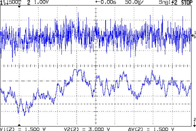
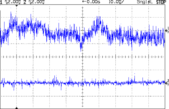
With that setup, the first LM324 with a gain of 10 produces this dismal result:
Op Amp 1 10x gain spectrum – 9-209 kHz
Past an op amp’s -3 dB cutoff, the response drops at 10 dB/decade for a while. Squinting at that curve, it’s down 10 dB at 40 kHz and the cutoff looks to be around 4 kHz… not the 100 kHz you’d expect from the GBW/gain number.
[Edit: You’d expect a 6 dB/octave = 20 dB/decade drop from a single-pole rolloff. That’s obviously not what’s happening here.]
The LM324 has a large-signal slew rate of about 0.5 V/µs that pretty well hobbles its ability to follow full-scale random noise components.
Both traces come from a kludged 10 dB AC coupled “attenuator” probe: a 430 Ω resistor in series with a 1 µF Mylar cap, jammed into a clip-lead splitter on the BNC cable to the analyzer. Probably not very flat, but certainly good enough for this purpose.
The SA is averaging 100 (which was excessive) and 10 (more practical) successive traces in those pix, which gives the average of the maximum value for each frequency bin. That reduces the usual hash you get from a full-frontal noise source to something more meaningful.
The LM317 tweaks the reverse bias voltage to ram about 10 µA of DC current through the 2N2907A base-emitter junction; I picked that transistor because it has a 5.0 V breakdown spec that translates into about +8 V in reality, plus I have a few hundred lying around.
The 4.7 kΩ collector resistor sets the operating point of the 2N3904 NPN transistor at a bit over 6 V with a collector current of 1.6 mA, around which there appears ±500 mV of pure noise:
Noise – NPN C inv – op amp
The 2N3904 spec says hFE > 100 and, indeed, I measure 200: 8 µA in, 1.6 mA out.
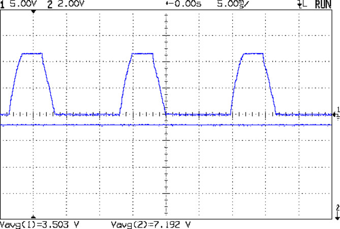
The bottom trace is the output of the first LM324. With a GBW of 1 MHz and a voltage gain of 10, it should have a cutoff at 100 kHz, but that’s obviously not true; the 0.5 V/µs large-signal slew rate just kills the response. The flat tops at 3.8 V show that it’s definitely not a rail-to-rail op amp.
The horizontal cursors mark the ATmega 328 minimum VIH and maximum VIL; the actual thresholds lie somewhere between those limits. What you don’t get is the crisp transition from a comparator.
The trimpot setting the logic level lets you tune for best picture; in this case, that means balancing the number of 0 and 1 bits. It’s a bit more complex, of course, about which, more later.
I picked the LM324 for pedagogic reasons; it’s a Circuit Cellar column and I get to explain how a nominally good analog circuit can unexpectedly ruin the results, unless you know what to look for…
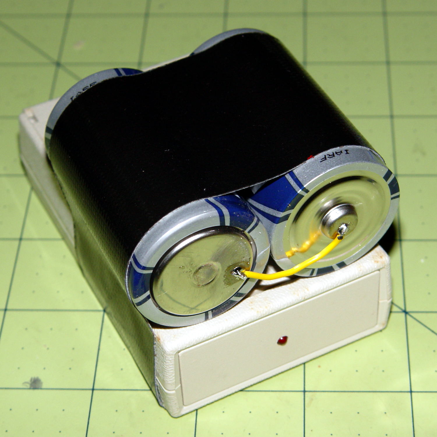
I duct-taped a pair of D cells onto the case and returned it to the bedroom shelf. According to the date scrawled on the tape, that was five years ago: 26 November 2010.
Over the last few months, the LED gradually faded from a blink to a steady glow as the battery voltage dropped below 2 V and the WWVB receiver output no longer reached the MOSFET’s threshold.
We’ll see how long these last:
Alpha Geek Clock – new batteries
Yeah, I should probably do something involving 3D printing…
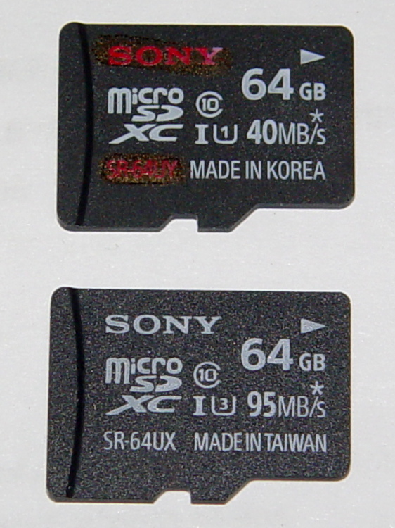
A little over a year ago, I bought two Sony 64 GB MicroSDXC cards (let’s call them A and B). Both cards failed after less than six months in service and were replaced under warranty with Cards C and D:
Sony 64 GB MicroSDXC cards – front
The top card (C) is the most recent failure, the bottom (D) is the as-yet-unused replacement for Card D. Note that the difference: SR-64UY vs. SR-64UX, the latter sporting a U3 speed rating.
Note that the failure involves the card’s recording speed, not its read-write ability or overall capacity. Card C still has its nominal 64 GB capacity and will store-and-replay data just fine, but it can’t write data at the 25 Mb/s rate required by the camera… which is barely a third of the card’s speed rating. Also note that the writing speed is always a minute fraction of the reading speed that you see on the card.
I use these in a Sony HDR-AS30V action camera on my bike, so it’s pure Sony all the way. Although I don’t keep track of every trip, I do have a pretty good idea of what happened…
In service: about 2015-07-10
Failed to record 1920×1080 @ 60 f/s video: 2015-09-22
In round numbers, that’s 70 days of regular use.
My NAS drive has room for about a month of video, depriving me of a complete record of how much data it absorbed, but from 2015-08-21 through 2015-09-22 there’s 425 GB from 25 trips in 30 days. Figuring the same intensity during the complete 70 days, it’s recorded 800 to 900 GB of data (including my verification test). With 60 GB available after formatting, that amounts to filling the card 14 times.
That’s reasonably close to the 1 TB of data I’d been estimating for the failures of Cards A and B, so these Sony cards reliably fail their speed rating after recording 750 GB, more or less, of data.
The simplest possible electrometer amplifier that might work:
Electrometer amp – LMC6081 schematic
The general idea is that the op amp will drive the (essentially) open-circuited inverting input to match the 2 V offset at the noninverting terminal, so that the output will stabilize above the LMC6081’s minimum useful output voltage (of about 1 V) and the gamma-ray pulses will go downward from there (it’s an inverting amp). The rebiasing network downstream from the output cap doesn’t appear in the hardware.
The small cap across the feedback resistor that would compensate / roll off the high-frequency response isn’t possible, unless you have a stockpile of teeny glass vacuum capacitors: the leakage resistance must be far more than 100 GΩ and my collection lacks anything like that. A Teflon-insulated gimmick capacitor wouldn’t be stable enough and would probably still leak crazy current.
Normal electrometer amps operate at essentially DC and amplify an actual current from the ionization chamber. In this case, the radiation level is zero, there’s no chamber current, I’m looking for small pulses generated by gamma ray events, and the amplifier must have reasonable AC response. It’s not clear that circuit can work, but it’s a starting point.
It turned into a hairball:
Electrometer Amp – 10 Gohm Rf
The LMC6081IN is socketed, with the inverting input pin bent outward and soldered to the flying junction of the 100 kΩ input / OMG resistor (which prevents inadvertent shorts from the 24 V chamber bias) and the glass-body feedback resistor. The socket sits end-on in a puddle of epoxy, so I can swap op amps as needed.
The 100 GΩ feedback resistor didn’t work well at all:
LMC6081 100 G – out – noninv level – matched
The lower trace shows the 10.2 VDC offset at the noninverting input, which is what it took to drive the output from near 0 V to the 11.4 V in the upper trace, with no proportional change in between. I replaced the schematic’s 1 MΩ / 220 kΩ resistors with the 20 turn trimpot shown in the photo in order to find that bias condition. Obviously, the op amp acts as an open-loop comparator, not a linear amplifier, and no amount of waiting for it to stabilize would change that outcome.
It’s possible the resistor has failed open, but, frankly, the difference between “100 GΩ” and “open circuit” probably doesn’t amount to much. Note, however, that there’s absolutely no 60 / 120 Hz interference or noise, which continues to surprise me; removing the shield cap and teasing the twiddlepot slams the output with a 60 Hz trapezoid:
LMC6081 100 G – out – noninv level
Swapping in a 10 GΩ resistor produced a smoothly changing output for biases between about 1 V and 8 V, so it’s behaving like an op amp should. Setting the non-inverting terminal to 8 V puts the output voltage at 6.3 V, which means the 10 GΩ resistor drops about 1.7 V to pull 170 pA from the inverting input (which is presumably at 8 V give-or-take a bit) and the chamber electrode. The LMC6081 spec says a maximum of 4 pA (for the I version, which is what I have), so:
My cleanliness isn’t up to par
The chamber delivers quite a bit more zero-radiation current than I expected
The op amp’s input got toasted despite my efforts toward a static-free installation
Hard to choose among those options, it is, indeed.
With the bias set to produce a 6 VDC output, the AC coupled signal doesn’t seem promising:
LMC6081 10 G Rf – out and Vplus in – AC 2 mV div
The lower trace is the bias voltage applied to the noninverting input, which looks reasonably clean. The sweep triggers from the power line; there’s still no 60 Hz interference.
All those flying components are, as you’d expect, microphonic beyond belief: jumping on the concrete basement floor produces a corresponding bounce in the trace that may be due to air currents or noise, for all I can tell. Even with the chamber sitting on a loose cloth pad, tapping the workbench produces 10 s of slowly decaying oscillation, admittedly at a much lower frequency than the noise in that trace.
A single gamma ray event producing an unreasonably high 10 fA chamber current will cause a downward (it’s an inverting amplifier) pulse that amounts to a mere 100 µV, a pulse that obviously isn’t visible against all that racket. You might convince yourself that the event at the center of the top trace comes from a gamma ray, but you’d probably be wrong.
In a normal electrometer amp, a stiff low-pass filter discards all the noise and isolates the DC signal corresponding to the steady-state chamber current from the ionizing radiation. Given that the pulses are on the order of 5 ms wide, there’s no obvious way to discard most of the noise without also tossing the signal.
Pending more thought, I’d say this was definitely fun while it lasted…
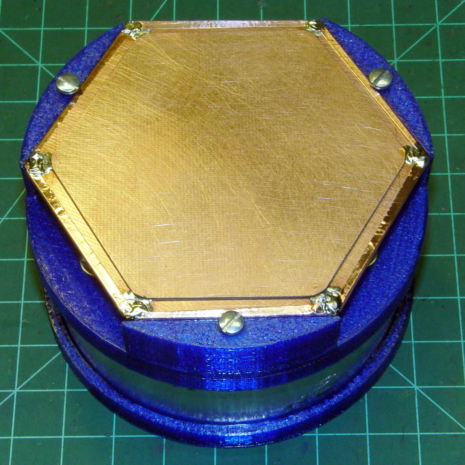
An undrilled double-sided circuit board with the edges bonded together doesn’t look like much:
Electrometer amp – undrilled shield planes
Soldering a smaller hex to the center of the bonded plate produces an isolated plane:
Electrometer amp – finished shield planes
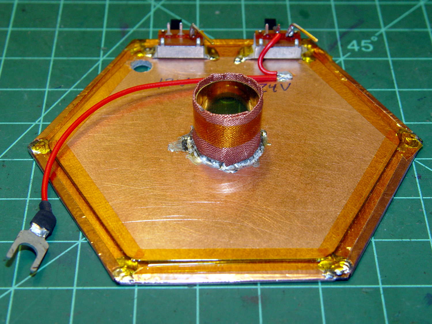
The copper fabric tape wrapped around a brass tube soldered to the isolated plane contacts the ionization chamber shell around the central contact and (should) provide complete shielding. Kapton tape around the edges reduces the likelihood of inadvertent shorts.
Working with a shield at +24 V gave me the shakes, so this one confines the chamber bias to the isolated hex and shell, with the larger hex at circuit common (a.k.a. ground). The isolated plane has about 275 pF to the ground plane, which isn’t a Bad Thing at all. In principle, the chamber bias doesn’t need a switch, because there’s no current drain, but I vastly prefer having cold circuitry before popping the lid.
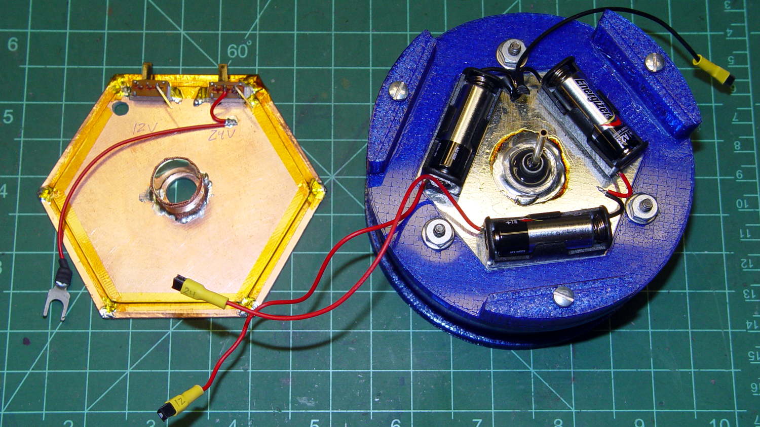
If I had a small DPST switch, I’d use it:
Electrometer amp – chamber – shield planes
As it stands, one switch controls the +24 V chamber bias and the other switches +12 V power to the electrometer amp front end, with simpleminded connectors so I can separate the pieces.
We’ll see how well all that works in practice.
An alert reader will notice the tiny difference between the blue PETG shapes in the two pictures. The bottom one comes from the revised code, of course.
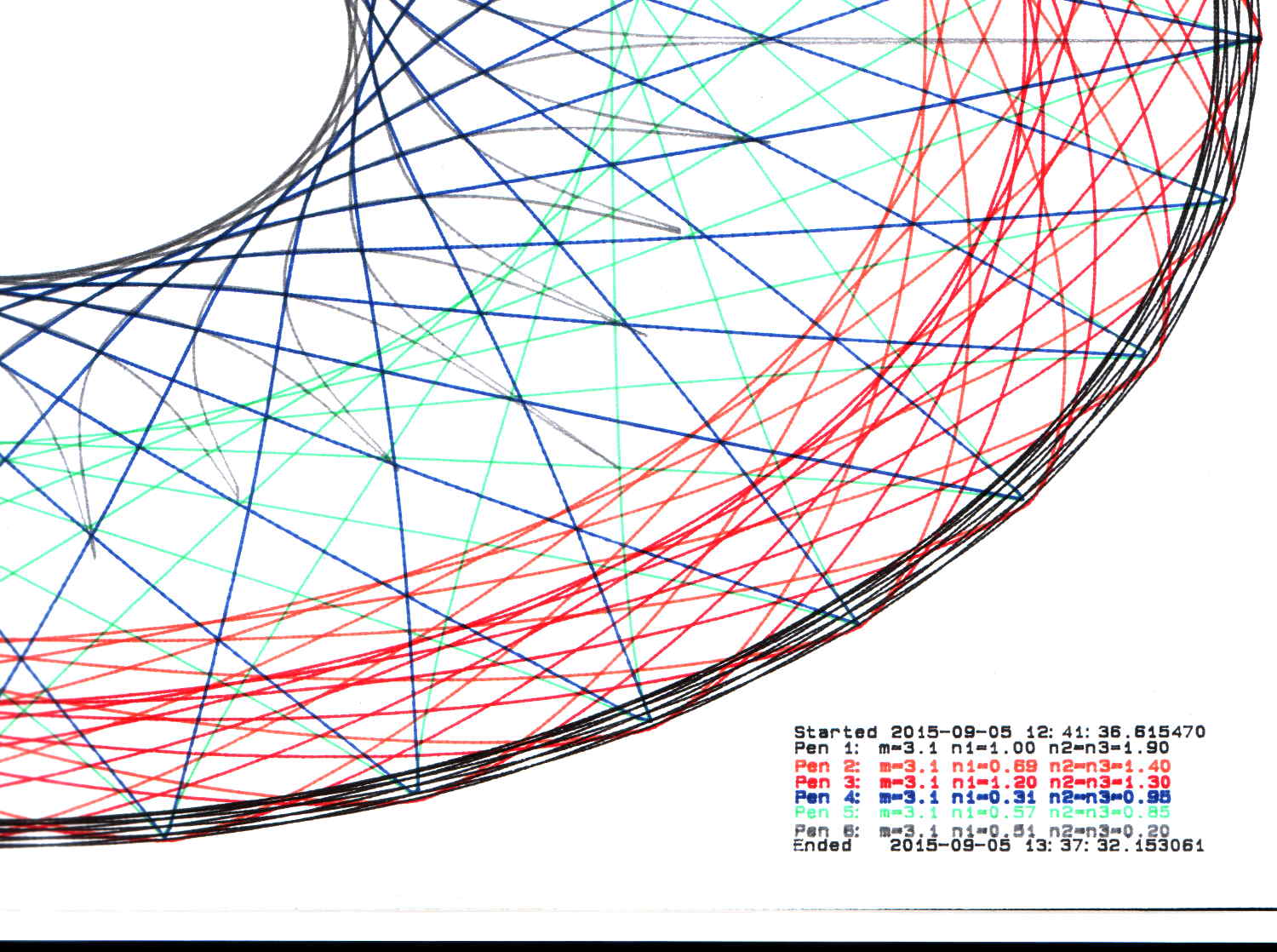
By now, I have half a dozen baggies each containing half a dozen plotter pens, plus a demo program that can produce good-looking Superformula plots, so I can do this without any hassle:
HP 7475A 2541A 68465 – Random pens
And this:
HP 7475A 2641V 26599 – Random pens
I must confess to not being good at withstanding temptation; the second plot comes from another HP 7475A plotter that I won on eBay:
Stacked HP 7475A Plotters
Apparently, nobody else wanted a plotter advertised as “non-working”, leaving me as the sole bidder. The photos showed that it powered up properly, sported a serial (not HPIB) interface, had an (empty) carousel with rubber pen boots (that were, oddly enough, not fossilized), and came with a complete set of manuals. Turns out any one of those items sells for more than the entire package, so I can part it out, flip the pieces, and Profit! if I were so inclined.
Load the carousel with a handful of restored pens, insert a sheet of paper, hold down the P1 + P2 buttons, flip the power switch, and out comes a perfectly drawn demo plot: