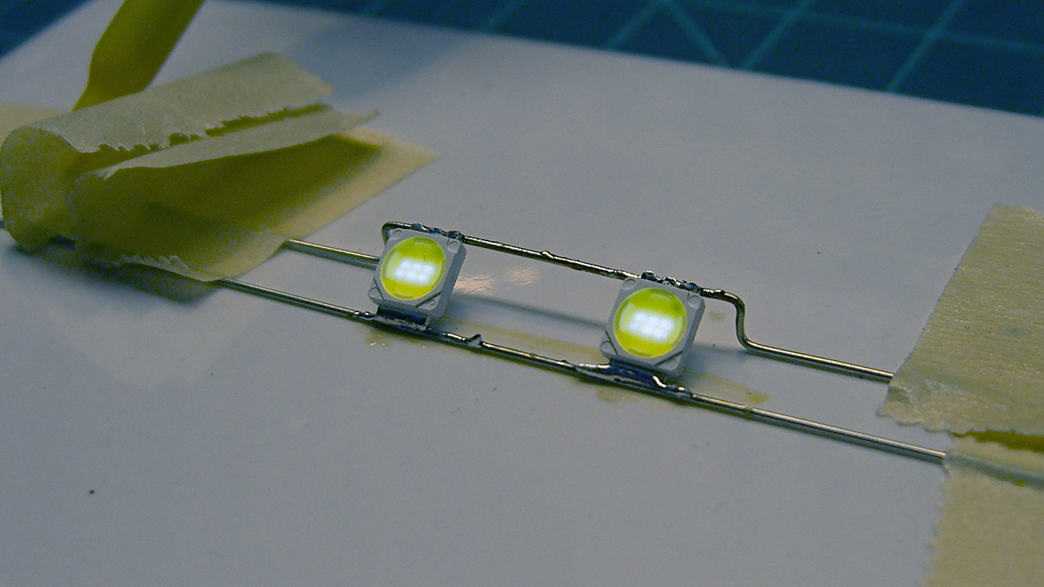
Each LED emitter in the Kenmore 158 endcap light contains six chips in series:
Even though the current has the usual exponential relationship to the terminal voltage, the slope at 200 mA (100 mA each, assuming they share & share alike) remains low enough that I (think I) can get away with just dialing in a voltage and leaving it at that; changes due to small temperature variations won’t cause meaningful differences in the current.
That’s easier than building an adjustable current regulator, anyway.
The heap disgorged two cheap DC-to-DC boost converters from halfway around the planet, with about the right specs:
- 10 to 32 V DC in
- 12 to 35 V out
- 10 A
- 150 W
They couldn’t produce their rated output, but a pair of LEDs shouldn’t pose much of a challenge.
So I wired one up to the bench supply, set it for 12 V, turned it on, and wham it maxed out the supply at 3 A with no load on the converter’s output.
Huh.
Adding a suitable load resistor brought the input current down, but the voltage adjustment trimpot didn’t have much effect and the bench supply would still wham hit 3 A with no provocation, so the load resistor didn’t actually make any difference. Eventually, I figured out that simply pressing my finger on the trimpot caused the output to vary wildly.
Given that fairly broad hint, this became obvious:

Evidently, I had used the other converter for the previous tests. Huh.
With that trimpot pin soldered in place, the converter worked fine. Eyeballometrically speaking, the LEDs seem bright enough at 100 mA total (50 mA each) for my purposes, which happens at 18-ish V. Dissipating only 2 W won’t require nearly as much heatsink as they’re presently mounted on, although I should wait for warmer weather before concluding that they’re doing OK while crammed inside the end cap.
Before declaring victory, I took a closer look at the board and found this mmm oversight:
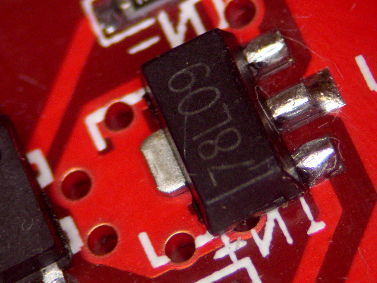
Notice the big pad under the 78L09 regulator, with six thermal vias to an expansive copper pour on the other side of the board, completely covered with red solder mask.
Removing the regulator show the regulator’s footprint didn’t include the tab:
Maybe they decided, after a careful analysis, that the regulator couldn’t possibly dissipate enough power to warrant the additional solder required for the entire thermal pad. Heck, pocket a fraction of a yuan on ten million boards and you’re livin’ large.
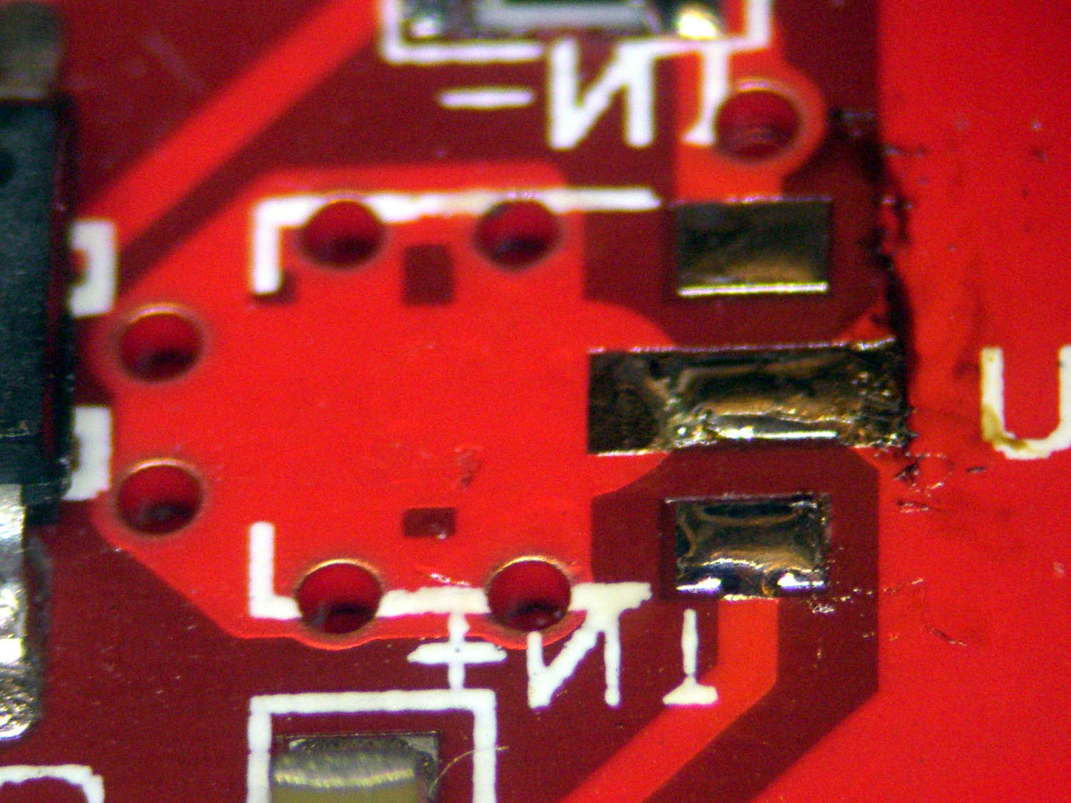
Scraping the mask off, fluxing everything in sight, and soldering the regulator down probably won’t make any difference:

Yes, The Bigger The Blob, The Better The Job strikes again. It does make me feel better and that’s all that counts.

Comments
6 responses to “DC-DC Boost Converter: Another QC FAIL”
Many ebay parts come from sources with which I’m extremely familiar — what markings, if any, are on that SOIC8 on the bottom, beside the 78L09?
(I’m making the possibly bad assumption that the chip on the bottom is the boost controller, and the TO220’s are the switches.)
In order to protect their IP (or cover their tracks), they sanded that chip clean…
The TO220s are IRF2807 and MBR2060CT: one FET, one dual rectifier. They have high production values and might actually be from IR and ON, respectively, but good laser work is cheap and readily available these days.
The serpentine PCB-trace inductor / resistor on the IRF2807 source lead might be diagnostic: either they have really good designers or it’s straight from the recommended layout.
[…] DC-DC boost power supply for the LED needle lights has four mounting holes, two completely blocked by the heatsink […]
It seems to me that many of those layouts are done by people who don’t really know what they are doing. A.k.a. cargo cult engineering. They look at the board and it is all the same to them.
If it weren’t for the PCB layouts in the data sheets and app notes, nothing would work…
I have that on high authority from a mole formerly planted high in a Noted Semiconductor Company. [grin]