The fact that changing R220 also changed the noise should have pinpointed the noise source, but such things are always more obvious in retrospect than in real time running. This post should help me start the next debugging spree a bit further up the learning curve.
The AM503 signal path includes a pair of … unique … differential amplifier ICs made by Tektronix back in the early days of integrated circuitry:
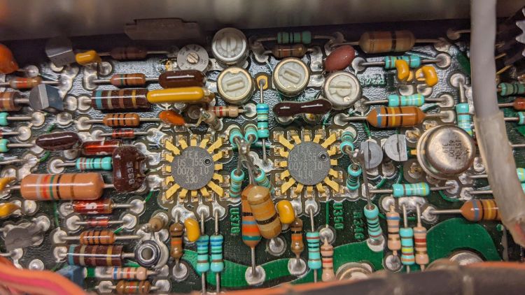
The picture has the signal flowing right-to-left through U350 and U370, starting with the Q310 dual NPN in the metal can and the Q315/325 PNP pair (both over on the right side near the cable).
The schematic goes left-to-right:

This AM503 PCB does not have the change that split Q310 into two separate transistors, as shown in the upper left of the schematic.
The single-ended input signal comes from Q230 at the output of the attenuator on the previous schematic page:
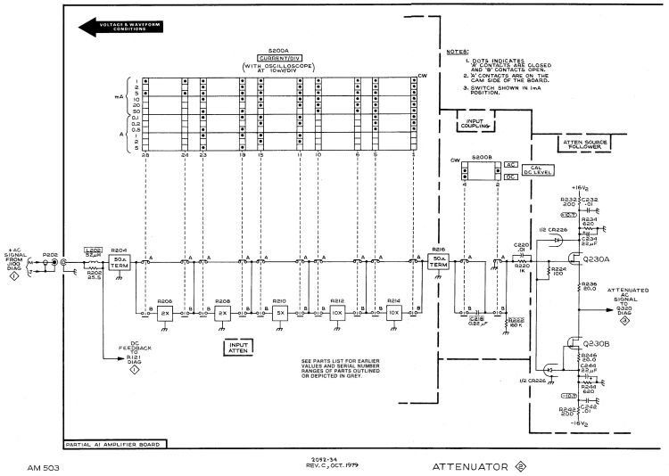
Here, U350 mashes the signal together with the DC offset control and makes it differential, U370 filters it, then Q390 produces a single-ended signal for the scope output. The architecture makes sense when you realize the AM503 started out as a mainframe oscilloscope plugin and became a TM500 plugin as the result of a mid-flight product pivot; think of it as the hardware version of technical debt.
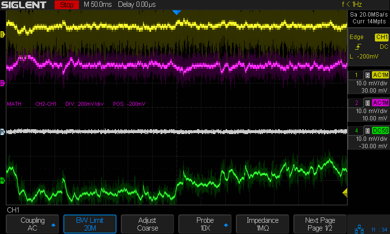
Anyhow, the differential output of U370 shows the noise across pins 6 and 8 (yellow and magenta):

Again in retrospect, pins 9 and 5 would have been a better choice.
The white line is the difference between the two pins and resembled the scope output in the bottom trace well enough to satisfy me.
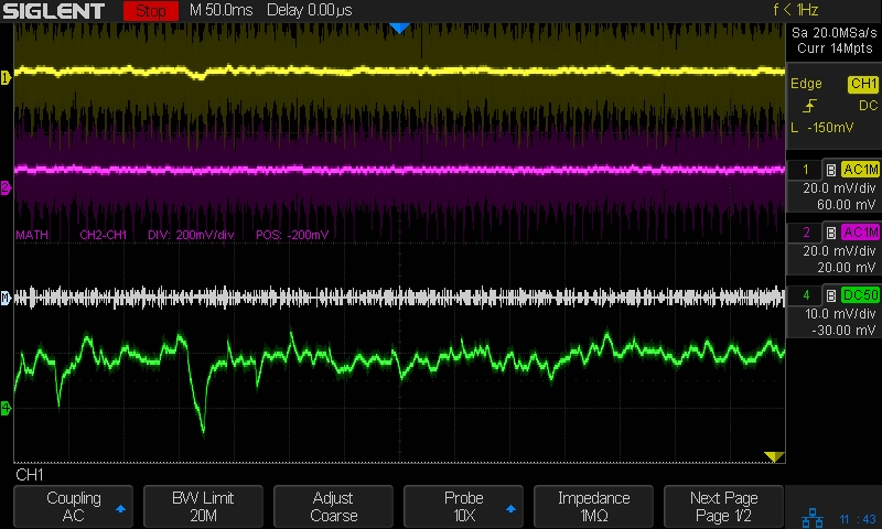
The differential input to U350 on pins 16 and 14 also shows a distinct similarity to the output noise:
It’s essentially impossible to snap a scope probe around those IC pins, but merely extraordinarily difficult to securely grab the tails of the pin sockets extending beyond the solder side of the PCB.
Finally, a look across R317, the emitter resistor between the halves of Q310:
That was enough to finally convince me the problem lay upstream of Q310.
Ruling out the DC level pot required balancing another AM503 atop this one to plug its cable into the PCB, which showed same output noise.
Hat tip to Sherlock Holmes:
“When you have eliminated all which is impossible, then whatever remains, however improbable, must be the truth.”
https://www.goodreads.com/quotes/1196-when-you-have-eliminated-all-which-is-impossible-then-whatever
Because Q230 is socketed, I pulled it out and popped it into another AM503, whereupon the noise followed the transistor:
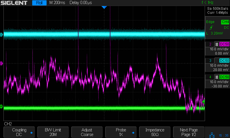
All three AM503 amps are set to GND / DC LEVEL CAL. The cyan trance is the formerly noisy amp (now with a good Q230), the magenta trace is the formerly good amp (now with the bad Q230) , and the green trace is the best of the three AM503 amps (untouched, for well and good reason) in my collection.
So I must replace a four decade old dual JFET sporting Tek part number 151-1032-00. Such things are available, but in rather grisly as-is condition or as New Old Stock collectibles.
Perhaps a middle ground would suffice? A couple of those should arrive in a while, but it’s not clear they’re a drop-in replacement.

Comments
One response to “Tektronix AM503: Noisy Q230 Dual JFET”
[…] a 2N5911 dual JFET into the noisy Tektronix AM503 (B064098) eliminated both the noise and the offset […]