This is the drilled and etched PCB for the brassboard of the Hall effect current control LED Blinky Light:
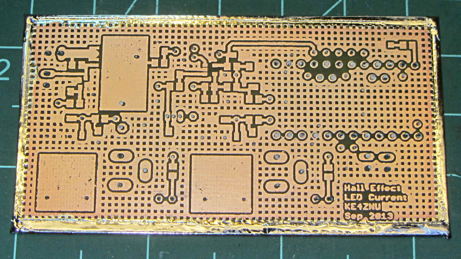
The big rectangle at the top will heatsink the main p-MOSFET power switch, which shouldn’t dissipate much power at all. The two lower rectangles heatsink the n-MOSFETs, although I think they may each require a stand-up metal tab to handle the dissipation during high-duty-cycle blinkiness.
The silver line around the edge is soldered copper foil tape connecting the top and bottom ground planes; a dozen or so additional Z wires will connect the planes at high current nodes. It’ll get a bunch of flying signal wires, too, because I’m not a fanatic gotta-embed-all-the-wires kind of guy on stuff like this.
The PCB is 30 mil FR4, which (once again, I make this mistake over and over again) seems a bit bendy for surface-mount parts; I must print a simple nest to stabilize the poor thing. Some of the drilled holes look white, because I hadn’t rinsed out the remains of the silver plating powder; the surfaces are a lot more silvery in person.
Before I etched the back side, I realized I’d made a classic layout blunder: the high-current return path from the center MOSFET flows around the Hall effect sensor near the center of the board. So I filled in the grid pour with a fat point black Sharpie to get more copper in that area:
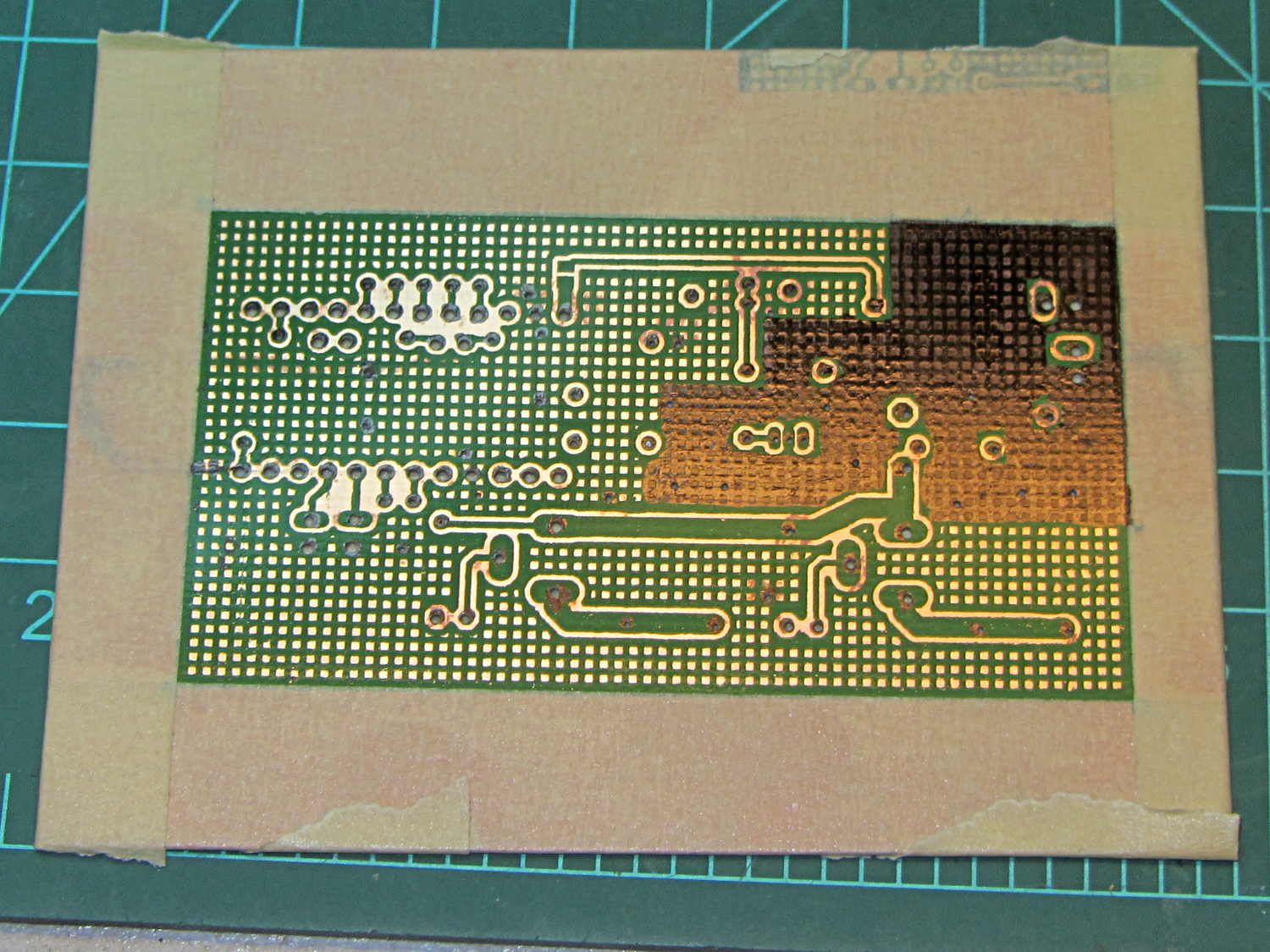
I think it probably wouldn’t matter either way, but nothing exceeds like excess. FWIW, I use the grid pattern as a way to verify the end of the board etching: when all the holes in the ground pour come clear, all the traces are done, too.
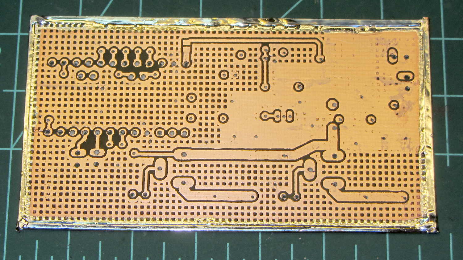
The etched backside came out OK, although with a few etched squares sprinkled in the Sharpie masking:
The three leads for the Hall effect sensor are just to the right of the center, with the middle lead connected to the ground pour. Given the millivolt-level signals, this isn’t a good place for ground bounce…
It’s etched with ferric chloride, rubbed with a sponge, and took under ten minutes on each side. That’s less than the usual time, which suggests the PCB is plated with half-ounce copper (that’s 0.5 ounce / ft2), rather than the one-ounce copper on the other boards I’ve done recently; just one of the hazards of buying surplus PCB stock. Doesn’t really matter, as the peak currents will be under half an amp and now I know not to use this batch of raw board stock for high current circuits.
All in all, it looks good enough. Now, for some component soldering.
