-
Measuring Objects for 3D Modeling: USB Video Camera
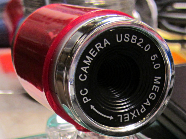
A brace of “Fashion” USB video cameras arrived from halfway around the planet. According to the eBay description and the legend around the lens, they’re “5.0 Megapixel”:
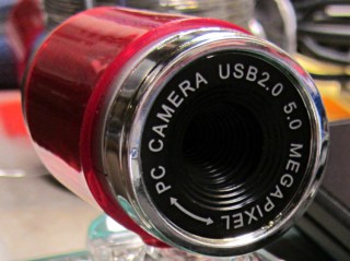
Fashion USB camera – case front The reality, of course, is that for five bucks delivered you get 640×480 VGA resolution at the hardware level and their Windows driver interpolates the other 4.7 megapixels. VGA resolution will be good enough for my simple needs, particularly because the lens has a mechanical focus adjustment; the double-headed arrow symbolizes the focus action.
But the case seemed entirely too bulky and awkward. A few minutes with a #0 Philips screwdriver extracted the actual camera hardware, which turns out to be a double-sided PCB with a lens assembly on the front:
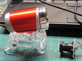
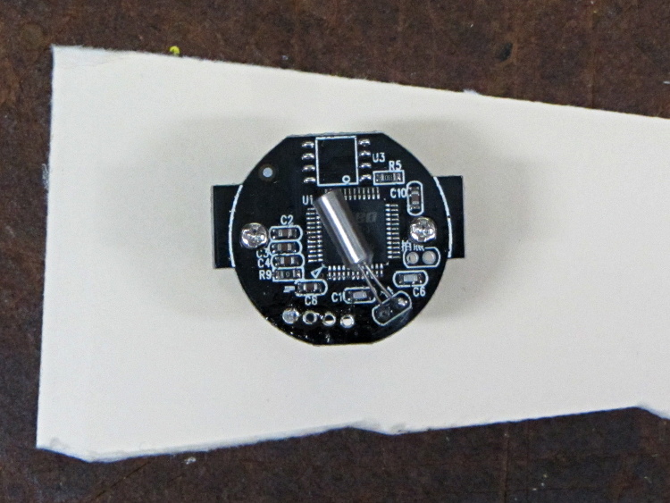
Fashion USB video – case vs camera The PCB has asymmetric tabs that ensure correct orientation in the case:
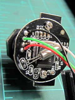
Fashion USB camera – wired PCB rear In order to build an OpenSCAD model for a more compact case, we need the dimensions of that PCB and those tabs…
Start with a picture of the back of the PCB against white paper, taken from a few feet to flatten the perspective:
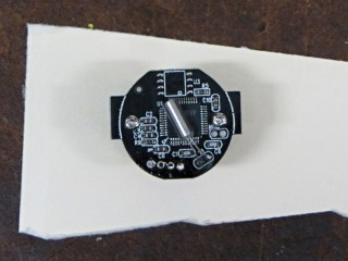
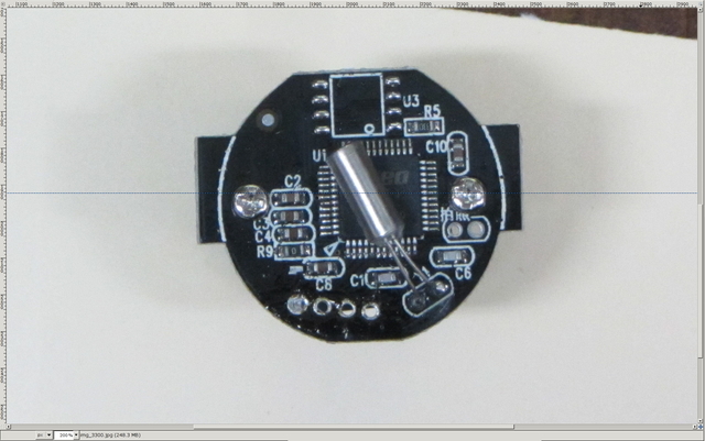
img_3300 – Camera PCB on white paper Load it into The GIMP, zoom in, and pull a horizontal guide line down to about the middle of the image:
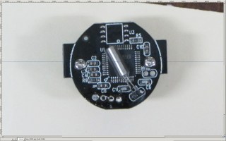
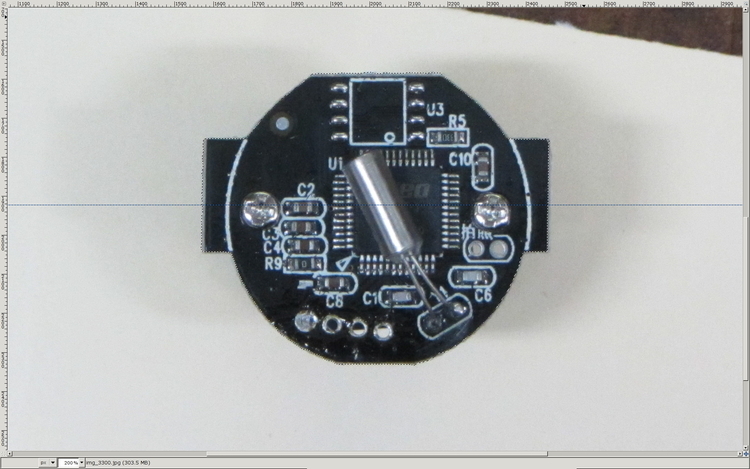
Camera PCB – horizontal guide – scaled Rotate to align the two screws horizontally (they need not be centered on the guide, just lined up horizontally):
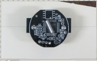
Camera PCB – rotated to match horizontal guide – scaled Use the Magic Scissors to select the PCB border (it’s the nearly invisible ragged dotted outline):
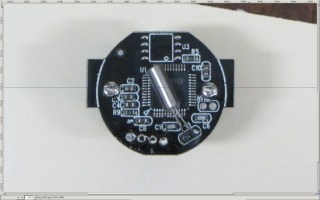
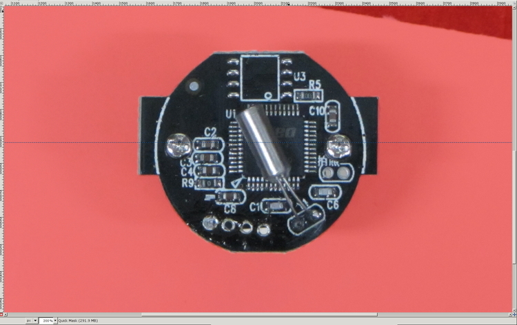
Camera PCB – scissors selection – scaled Flip to Quick Mask mode and clean up the selection as needed:
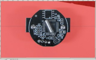
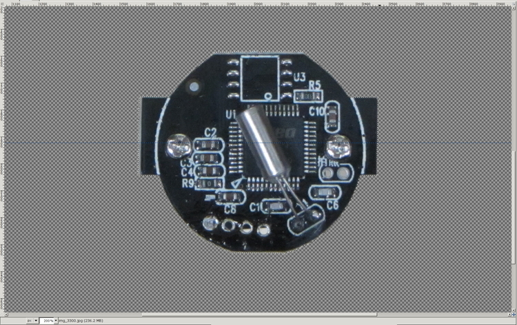
Camera PCB – quick mask cleanup – scaled Flip back to normal view, invert the selection (to select the background, not the PCB), and delete the background to isolate the PCB:
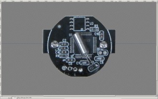
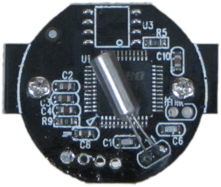
Camera PCB – isolated – scaled Tight-crop the PCB and flatten the image to get a white background:
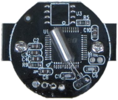
Camera PCB – isolated – scaled Fetch some digital graph paper from your favorite online source. The Multi-color (Light Blue / Light Blue / Light Grey) Multi-weight (1.0×0.6×0.3 pt) grid (1 / 2 / 10) works best for me, but do what you like. Get a full Letter / A4 size sheet, because it’ll come in handy for other projects.
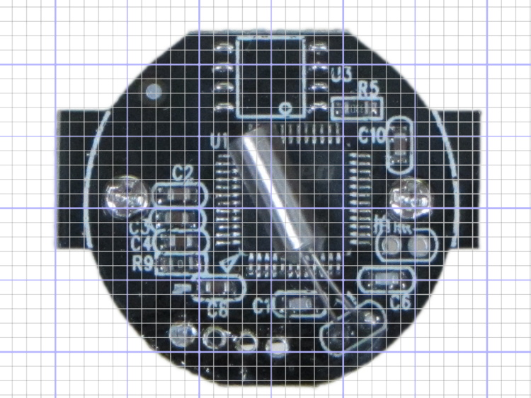
Open it up (converting at 300 dpi), turn it into a layer atop the PCB image, use the color-select tool to select the white background between the grid lines, then delete the selection to leave just the grid with transparency:
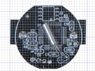
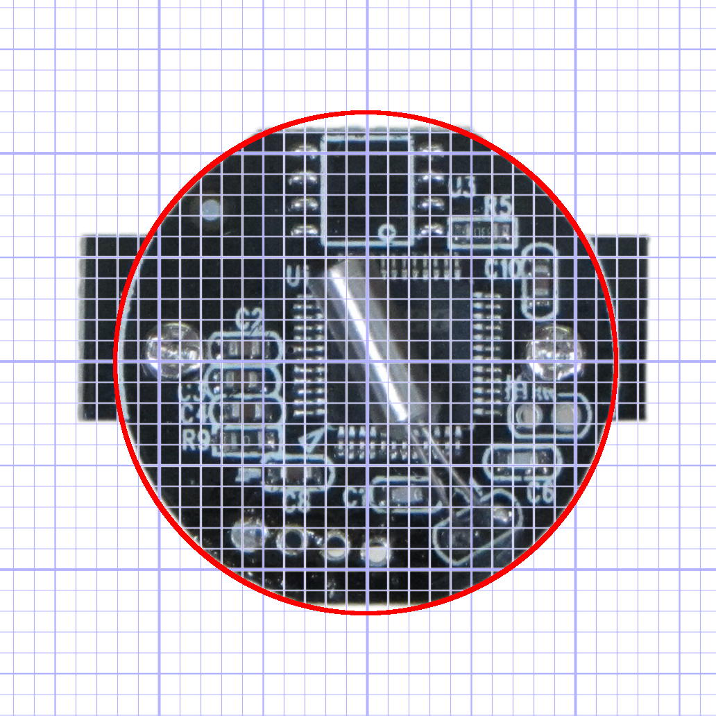
Camera PCB with grid overlay – unscaled We want one minor grid square to be 1×1 mm on the PCB image, sooo…
- Accurately measure a large feature on the real physical object: 27.2 mm across the tabs
- Drag the grid to align a major line with one edge of the PCB
- Count the number of minor square across to the other side of the image: 29.5
- Scale the grid overlay layer by image/physical size: 1.085 = 29.5/27.2
- Drag the grid so it’s neatly centered on the object (or has a major grid intersection somewhere useful)
That produces a calibrated overlay:
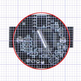
Camera PCB with grid overlay Then it’s just a matter of reading off the coordinates, with each minor grid square representing 1.0 mm in the real world, and writing some OpenSCAD code…



-
Subscribe
Subscribed
Have a WordPress.com account? Log in now.

