Ed Nisley's Blog: Shop notes, electronics, firmware, machinery, 3D printing, laser cuttery, and curiosities. Contents: 100% human thinking, 0% AI slop.
My buddy Eks asked me to help fix his new-to-him and guaranteed broken Tek 492 spectrum analyzer, which turned into a tour-de-force effort. One sub-project involved sucking the bits out of an existing “known-good” Tek memory card, which meant building a backplane connector and a circuit that behaved like a 6800 microcontroller… fortunately, it could be a lot slower.
[Update: It seems searches involving “Tektronix 492” produce this page. You may also be interested in these posts…
The HEX files you’ll need to replace failed ROMs and EPROMs
If those aren’t what you’re looking for, note that the correct spelling is “Tektronix“.
Good luck fixing that gadget: it’s a great instrument when it works!]
You can tell just by looking that this board was designed back in the day when PCB layout involved flexible adhesive tape traces and little sticky donut pads. Ground plane? We don’t need no stinkin’ ground plane!
Actually, it’s a four-layer board done with the usual Tek attention to detail. They didn’t need a ground plane because they knew what they were doing. Remember, this is in a spectrum analyzer with an 18-GHz bandwidth and 80 dB dynamic range; a little digital hum and buzz just wouldn’t go unnoticed.
Tek 492 Backplane Geometry
Anyhow, the backplane pins are on a 0.150-inch grid within each block. The center block (pins 13-36) is 0.200 inches from the left block (pins 1-12) and 0.250 from the right block (pins 37-60).
That means the left and right blocks are neatly aligned on the same 0.150-inch grid, with the middle block offset by 50 mils. You can’t plug the board in backwards unless you really work at it.
Of course, Eks had some genuine gold-plated Tek pins in his stash: 24 mils square and 32 mils across the diagonal. They have 1/4″ clear above the crimped area that anchors them to the black plastic spacer and are 1/2″ tall overall. They’re not standard header pins, but I suspect you could use some newfangled pins in a pinch.
Here’s what the reader board finally looked like, hacked traces and all, with the board connector to the rear. The memory board didn’t use all the backplane pins, so I only populated the ones that did something useful. The power-and-ground pins (left side of right pin block) stand separately from the other because I had to solder them to both the top and the bottom of the board: no plated-through holes!
Tek 492 Memory Board Reader
I cannot imagine this being useful to anybody else, but I defined an Eagle part for the connector so I could CNC-drill the board. Drop me a note and I’ll send it to you.
I’m doing some work with a one-off ROM reader & EPROM programmer, so it’s once again time to mess around with Intel HEX files, raw binary images, and the like.
The key routine (which runs on an Arduino Decimila) to dump a ROM in HEX format goes like this, with all the constants & variables & functions doing the obvious things:
void DumpHC641(void) {
word Address,Offset;
byte DataRd,Checksum;
for (Address = 0; Address < ROM_SIZE; Address += IHEX_BYTES) {
sprintf(PrintBuffer,":%02X%04X00",IHEX_BYTES,(word)Address); // emit line header
Serial.print(PrintBuffer);
Checksum = IHEX_BYTES + lowByte(Address) + highByte(Address) + 0x00; // record type 0x00
for (Offset = 0; Offset < IHEX_BYTES; ++Offset) {
digitalWrite(PIN_HEARTBEAT,HIGH);
DataRd = ReadHC641(Address + Offset);
digitalWrite(PIN_HEARTBEAT,LOW);
Checksum += DataRd;
sprintf(PrintBuffer,"%02X",DataRd); // data byte
Serial.print(PrintBuffer);
}
Checksum = -Checksum; // two's complement
sprintf(PrintBuffer,"%02X",Checksum);
Serial.println(PrintBuffer);
}
Serial.println(":00000001FF"); // emit end-of-file line
}
So getting an Intel HEX file is just a matter of capturing the serial output, whacking off any debris on either side of the main event, and saving it.
The srec_cat program handles conversions among a myriad formats, most of which I can’t even pronounce. The few I use go a little something like this:
It’s sometimes handy to apply srec_cat to a group of similarly suffixed files, in which case some Bash string chopping comes in handy. For example, to convert some hex files into binary:
for f in 27HC641*hex ; do echo ${f%%hex} ; srec_cat "$f" -intel -o "${f%%hex}"bin -binary ; done
Good old diff works fine on text files, but in this case it’s better to see which bytes have changed, rather than which lines (which don’t apply in the context of a binary file). The vbindiff program looks great on a portrait-mode display.
I don’t do much binary editing, but tweak serves my simple needs. Confusingly, members of this class of program are called “hex editors”, but they really work on binary files.
There’s also diff3, for those rare cases where you must mutually compare three text files. Makes my head spin every time…
All those programs are likely packages in your favorite Linux distro.
Quite often, the values you need for voltage regulators, like the venerable LM317 and its ilk, don’t work out to anything you have in your parts bin. What to do?
One of the really nice things about SMD resistors is that you can stack them up without much effort. That parallels their value, so you can only make the final value smaller than any of the stacked resistors, but we can work with that.
The schematic shows part of a multi-voltage power supply for the EPROM programmer I mentioned there. Normally you use a 240-Ω resistor between the Output and Adjust terminals, but anything in that range will work fine. Alas, when I went to the parts bin, that’s the value I didn’t have any of.
But, having recently acquired an assortment of 60-some-odd 1% chip resistors, 100 to the bag, I had enough raw material to make it work. In fact, the values in the schematic reflect the parts on hand, which is how it sometimes happens.
A pair of 499-Ω resistors in parallel gives you 249.5 Ω, close enough to 240 (and shown as 250 because that’s only 0.2% off). Plug that value and the desired voltages into the LM317 equation to find the other resistors:
12.5 V = 1.25 * (1 + R / 250)
R = 250 * ((12.5 / 1.25) – 1) = 2250 Ω
If you happen to have something close to that in your parts heap, great. I didn’t, and a stock 2200 Ω 5% resistor would produce 12.25 V; a bit lower than I wanted.
Three sets of stacked chip resistors
This pic shows the solution: stack some SMD resistors to get the right value.
To make this work easily, you need a calculator that has a reciprocal (1/x or x-1) key. My ancient HP-48 does that, natch, but both of the Official School Calculators our daughter uses has 1/x as a shifted function. Your mileage will certainly vary.
Anyhow, the reciprocal of the resistance of two parallel resistors, RA and RB, is the sum of their reciprocals. Got that?
1/R = 1/RA + 1/RB
If you know the total resistance R that you want and one of the resistors RA, then you find the other resistor RB thusly:
1/RB = 1/R – 1/RA
In order to get 2250 Ω, I started with the next higher value in the assortment, 2740 Ω, and turned the crank:
1/RB = 1/2250 – 1/2740 = 79.4809E-6
RB = 1/79.4809E-6 = 12.58 kΩ
As it happens, the assortment didn’t have that value, either, but it did have 15 kΩ. The parallel resistance of 2740 and 15 k is:
2317 = 1 / (1/2740 + 1/15000)
So turn the crank one more time to find the third resistor RC:
1/RC = 1/2250 – 1/2317 = 12.814E-6
RC = 78.04 kΩ
Well, that isn’t one of the values I have either, but I do have 82.5 kΩ. The parallel value of those three resistors is:
1/R = 1/2740 + 1/15000 + 1/82500 = 443.75E-6
R = 2254 Ω
Which is 0.1% off the desired value. Close enough.
Actually, it won’t be nearly that close, because the 2740 Ω resistor can be off by 27 Ω either way. If you really care, measure the actual values and feed those into the equations. If, of course, you can measure resistors better than 1% and you don’t care about temperature effects and suchlike.
This is appropriate for one-off projects and prototypes, not production runs, but it’s a handy trick to keep in mind. If you want to be fancy, you can lay the circuit board out with parallel resistor tracks and make it look like you knew what you were doing all along…
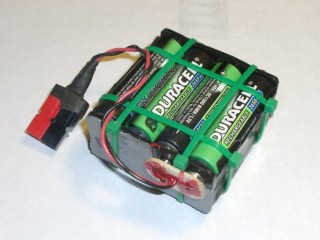
I’ve bought plenty of batteries from batteries.com over the years, but the alkaline AA cells I picked up last year have been a real disappointment: some had very short service lives. It took quite a while to figure this out, as I mentioned there, and when I finally got around to checking the rest of the package, most of them were dead… in Spring 2009 with a 12-2012 date code.
One characteristic of the weak / dead cells is that the negative terminal is swollen, even on the deaders direct from the package. This picture shows four cells removed from service: the front two are used with some remaining charge, the rear two are dead.
When I checked the package, most of the dead-on-delivery cells had swollen bottoms, so I suspect they had a manufacturing problem with at least one batch of cells.
A query to batteries.com asking about this got no reply. Perhaps they were busy dealing with the aftermath of their security breach?
A 48-pack of alkaline cells from the late Circuit City, bought about the same time, seems just fine.
Many interesting projects require more digital output bits than the Arduino hardware can support. You then use 74HC595 serial-in/parallel-out chips and that tutorial pretty well explains how it works. The shiftOut() library function squirts a byte out through an arbitrary pin, leading with either the high or low bit.
Software SPI: Clock and Data
Just drop one byte into shiftOut() for each ‘595 lined up on your board. Remember to latch the bits (LOW-to-HIGH on RCK @ pin 12 of the ‘595) and enable the output drivers (LOW on -G @ pin 13, similarly) when you’re done sending everything. You can have separate latches-and-enables for each ‘595 if that suits your needs, although then you once again run out of Arduino bits pretty quickly. It’s entirely possible to devote a ‘595 to latches-and-enables for the rest of the chain, but that gets weird in short order.
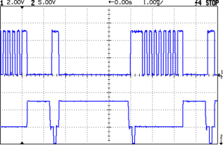
The scope shot shows that shiftOut() ticks along at 15 µs per bit (clock in the upper trace, data in the lower trace). For back-of-the-envelope purposes, call it 8 kB/s, which is probably less than you expected. If you have a string of 5 external bytes, as I did on a recent project, that’s only 1600 updates / second. It was part of a memory board reader & EPROM programmer: reading an 8 kB ROM chip requires two shift-register runs (one to set the address & data, one to read in the chip output), so the overall rate was on the order of 10 seconds per pass and much worse for programming. You can optimize the number of bits by not shifting out all the bytes, but that’s the general idea.
Because ‘595 chips are output-only, in order to get 8 bits of data into the Arduino board, add a 74HC166 parallel-in/serial-out chip to the string. Alas, shiftOut() doesn’t know about input bits, so you’re on your own.
Hardware SPI: Clock and Data
If you’re going to have to write some code to get input bits anyway, you may as well use the ATmega168 (and its ilk) hardware SPI as it was intended to be used: for high-speed synchronous serial I/O. This scope shot shows the SPI clock (in the top trace again) ticking along at 1 µs per bit, which is 1/16 the Diecimila’s oscillator frequency. You can pick any power of two between 1/2 and 1/128; I used 1/16 because it’s fast enough to make the rest of the software the limiting factor, while slow enough to not require much attention to layout & so forth.
Start by Reading The Fine Manual section about the ATmega168’s SPI hardware, starting at page 162.
The pin definitions, being lashed to internal hardware, are not optional. Note that SCK is also the standard Arduino LED, which won’t be a problem unless you need a tremendous amount of drive for a zillion ‘595s. I stuck an additional LED on Arduino digital pin 2.
#define PIN_HEARTBEAT 2 // added LED
#define PIN_SCK 13 // SPI clock (also Arduino LED!)
#define PIN_MISO 12 // SPI data input
#define PIN_MOSI 11 // SPI data output
Initial hardware setup goes in the usual setup() function:
pinMode(PIN_SCK,OUTPUT); // set up for "manual" SPI directions
digitalWrite(PIN_SCK,LOW);
pinMode(PIN_MOSI,OUTPUT);
digitalWrite(PIN_MOSI,LOW);
pinMode(PIN_MISO,INPUT); // configure inputs
digitalWrite(PIN_MISO,HIGH);
SPCR = B01110001; // Auto SPI: no int, enable, LSB first, master, + edge, leading, f/16
SPSR = B00000000; // not double data rate
Basically, the “manual” setup allows you to wiggle the bits by hand with the hardware SPI control disabled.
Arduino Hardware SPI Schematic
Here’s a chunk of the schematic so you can see how the bits rattle around. You’ll surely want to click it to get the details…
I put the data in a structure that matches the shift register layout, with the first byte (Controls) connected to the ATmega’s MOSI pin and the last byte (DataIn) connected to MISO. The SCK pin drives all of the serial clock pins on the ‘595 and ‘166 chips in parallel. Your structure will certainly be different; this was intended to suck data from a Tek 492 Spectrum Analyzer memory board.
typedef struct { // external hardware shift register layout
byte Controls; // assorted control bits
word Address; // address value
byte DataOut; // output to external devices
byte DataIn; // input from external devices
} SHIFTREG;
SHIFTREG Outbound; // bits to be shifted out
SHIFTREG Inbound; // bits as shifted back in
The functions that make it happen are straightforward:
void TogglePin(char bitpin) {
digitalWrite(bitpin,!digitalRead(bitpin));
}
void PulsePin(char bitpin) {
TogglePin(bitpin);
TogglePin(bitpin);
}
void EnableSPI(void) {
SPCR |= 1 << SPE;
}
void DisableSPI(void) {
SPCR &= ~(1 << SPE);
}
void WaitSPIF(void) {
while (! (SPSR & (1 << SPIF))) {
// TogglePin(PIN_HEARTBEAT); // use these for debugging!
// TogglePin(PIN_HEARTBEAT);
continue;
}
}
byte SendRecSPI(byte Dbyte) { // send one byte, get another in exchange
SPDR = Dbyte;
WaitSPIF();
return SPDR; // SPIF will be cleared
}
void CaptureDataIn(void) { // does not run the shift register!
digitalWrite(PIN_ENABLE_SHIFT_DI,LOW); // allow DI bit capture
PulsePin(PIN_SCK); // latch parallel DI inputs
digitalWrite(PIN_ENABLE_SHIFT_DI,HIGH); // allow DI bit shifting
}
void RunShiftRegister(void) {
EnableSPI(); // turn on the SPI hardware
Inbound.DataIn = SendRecSPI(Outbound.DataIn);
Inbound.DataOut = SendRecSPI(Outbound.DataOut);
Inbound.Address = SendRecSPI(lowByte(Outbound.Address));
Inbound.Address |= ((word) SendRecSPI(highByte(Outbound.Address))) << 8;
Inbound.Controls = SendRecSPI(Outbound.Controls);
PulsePin(PIN_LATCH_DO); // make new shift reg contents visible
PulsePin(PIN_LATCH_ADDRESS);
PulsePin(PIN_LATCH_CONTROLS);
DisableSPI(); // return to manual control
}
Actually using the thing is also straightforward. Basically, you put the data-to-be-sent in the Outbound variables and call RunShiftRegister(), which drops output bytes into SPDR and yanks incoming bytes out, then stuffing them in the Inbound variables. I have separate latch controls for the Controls, Address, and Data chips, although I don’t use them separately here.
You must wiggle the parallel latch enable line on the 74HC166 chip before shifting to capture the data, as shown in CaptureDataIn(). That chip also requires a separate pulse on its serial clock line to latch the data, which you do manually with the hardware SPI disabled. If you’re paying attention, you’ll wonder if that clock pulse also screws up the data in the rest of the chips: yes, it does. If this is a problem, you must add some external clock-gating circuitry, disable the ‘595s, or pick a different input shift register chip; it wasn’t a problem for what I was doing.
Here’s a function that reads data from a RAM chip on the Tek memory board, so it must write the address and read the RAM chip’s output. The PIN_DISABLE_DO bit controls the output buffers on the ‘595 that drives the RAM’s data pins; they must be disabled to read data back from the RAM. Don’t worry about the other undefined bits & suchlike; just assume everything does what the comments would have you believe.
byte ReadRAM(word Address) {
digitalWrite(PIN_DISABLE_DO,HIGH); // turn off data latch output
digitalWrite(PIN_BUS_READ,HIGH); // allow RAM read access
Outbound.Controls |= CB_BUS_CLKPH2_MASK; // set up RAM -CS gate
Outbound.Address = Address;
Outbound.DataOut = 0x55; // should not be visible
RunShiftRegister();
digitalWrite(PIN_BUS_N_SYSRAM,LOW); // activate RAM -CS
CaptureDataIn(); // latch RAM data
digitalWrite(PIN_BUS_N_SYSRAM,HIGH); // ... and turn -CS off
Outbound.Controls &= ~CB_BUS_CLKPH2_MASK; // disable -CS gate
RunShiftRegister(); // tell the board and get data
return Inbound.DataIn;
}
Hardware SPI – Detail of clock and data timing
Here’s a detailed shot of the outbound bit timing. Notice that the upward clock transitions shift bits into the ‘595 and ‘166 chips, while the SPI output data changes on the downward transitions. You can tweak that to match your hardware if you’re using different shift register chips, by messing with the SPCR settings.
Bottom line: using the ATmega168 hardware SPI provided a factor-of-15 speedup and serial digital input, too.
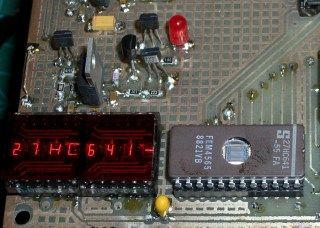
My buddy Eks recently acquired a “guaranteed broke” Tektronix 492 spectrum analyzer that turned out to have a defunct memory board: the ROM holding the initial boot firmware has a bad checksum. He verified that by swapping in a memory board from another 492 and found it worked perfectly.
The original board used Mostek MK36400 8Kx8 masked ROMs, but they can be replaced by either 27HC641 or (in a pinch) a quartet of 2716 EPROMs. Being a stickler for authenticity, Eks picked up some 27HC641 chips. That means we need a device programmer, as none of the burners we have know anything about 27HC641s. There are other ways of getting the job done, but this has the advantage of getting me some face time with my role model for being a Renaissance Man.
Tek EPROM Power Supply Breadboard
To make a long story somewhat shorter, the 27HC641 is a 8Kx8 EPROM in a 24-pin package with the usual 12 address lines, 8 data lines, power, ground, and a single chip-select / output-enable / programming-voltage pin. Normal EPROMs in 28-pin packages have separate pins for all those functions to make life easier.
Anyhow, the CE/VPP supply must provide 30 mA at 12.5 V as well as the usual minuscule FET logic currents at 5 V and 0 V. The VCC supply must cough up a staggering 90 mA during normal operation at 5 V and 30 mA at 6 V during programming. Both supply voltages must switch between three levels: unnaturally high during programming, 5 V for normal operation, and 0 V for output-enable and during chip removal / installation in the programming socket.
This being an entirely one-off project, I used good old LM317T regulators with a handful of transistor switches to vary the voltage and clamp the output to ground. The CE/VPP supply looks like this:
Schematic of VPP-VCE pin supply
An Arduino will drive the gates of Q2 & Q3, with all the programming logic and timing handled by software. The shortest VPP pulse is a millisecond long, so that’s not a real restriction, and the verification can happen at nose-pickin’ speed. That simplifies a lot of other things about the project, too.
Switch: 12.5 to 5 V
Q3 selects the output voltage: gate high = 5 V, gate low = 12.5 V. The scope shot shows the gate driven with a 500-Hz square wave, which is about the right width for the programming pulse.
I prototyped this on a solderless breadboard (ptooie) as shown above with 5% resistors, so the actual voltages aren’t quite nominal. The readout says 13.28 and 5.3 V, which will need some trimming to get inside the EPROM’s 5% spec.
The 1 nF cap at the LM317 Adjust terminal encourages stablity by knocking off the high-frequency stuff and slowing down the transitions just a smidge. The datasheet suggests up to 10 µF, which turns the transitions into triangles.
The LM317 can only supply current to its load, so reducing the output voltage requires the load to draw current from C3. Because this is essentially a DC application, C3 can be quite small: there won’t be any other switching going on during the programming pulse. The datasheet recommends 1 – 10 µF, but definitely more than 5 nF.
The LED is actually a key part of the circuit, as it draws current to pull the output voltage downward: more LED current = faster transition time. However, higher C3 = slower transitions.
Fall time: 12.5 to 5 V
Seen at a higher magnification, the falling edge of the output waveform shows a decay that lasts 50 µs or so. The LED draws maybe 12 mA at 13 V, so the voltage across C3 should drop at
(1/100 nF) x (12 mA) = 120 V/ms
Applying a straightedge to the early part of that curve looks like 25 V in 100 µs; call it 250 V/ms, maybe a bit less.
What’s a factor of two among friends, particularly given the tolerances on ceramic caps?
T1 and Q1 (I don’t know why Eagle’s models use both T and Q as transistor prefixes, it’s probably an international thing) switch the output line between the LM317 and ground; I suspect just turning T1 off would work as well, but this way the chip pin is firmly held to 0 V, where it should be, regardless of leakage and other oddities.
Switch: 5 to 0 V
Because Q1 crops both sides of the transistion, the rise and fall happen in nanoseconds rather than microseconds.
So, now that I know this will actually work, I can build a PCB and write some firmware…
Memo to Self: make sure the code waits for the output transitions. Methinks delayMicroseconds() will be a constant companion.
A friend brought over a broken toy (well, an Argent GPS tracker) with a peculiar problem: everything worked, but after a few minutes the front-panel LEDs would get intermittent. The LEDs are hand-soldered to the board with leads that extend maybe 7 mm from the surface.
After a bit of poking around, I stuck the gadget under the microscope, at which point the problems became obvious.
See that distinct line where the solder meniscus ends at the lead? Yup, that’s the teltale sign of a cold solder joint. The lead never got hot enough to bond properly with the solder, so the failure extends all the way down through the board. The only electrical contact is at a random point where the flux layer is thin enough to pass current; as the joint heats up, that point Goes Away.
Worse, do you see (click on the pix for bigger images) the small discontinuity about 1/3 of the way down the solder cone? My buddy Eks alerted me to that failure: that’s where the solder joint fractures from repeated heat stress.
Solder Thermal Stress
Here’s the quick sketch he drew on the canonical back-of-the-envelope. I added the red oval as a replacement for his emphatic gestures; with any luck, you’ll never forget it, either.
In this case the LED is anchored in a front-panel hole and the lead is mechanically locked to the board. As the lead heats & cools, it expands & contracts (duh) at a slightly different rate than the solder. After a while, the solder cracks; it’s much less ductile than copper.
Joint 2 – clear fracture
I’m not convinced that’s what happened here, as the LED leads have a bend in the middle that should relieve the stress, but it’s at exactly the spot where he sketched the failure he’s found in many, many gadgets. Power transistors standing above boards with their backs screwed to heatsinks seem particularly prone to this failure, as they have short leads stressed by the differential expansion between copper and aluminum.
Here’s another LED lead from the same gadget. A random out-of-focus fiber enters from the right and exits around to the left rear, but you can clearly see the bad joint at the top of the solder cone and the fracture line just below the fiber.
A touch of the soldering iron generally solves the problem, although you might want to suck the old solder out so the new solder can re-flux the joint.
Arduino Pro USB (cold) Solder Pads
This doesn’t happen only to hand-soldered joints. The USB header fell right off an Arduino Pro board while I was debugging something else. I had to re-heat the joints and the header separately, add flux, and then solder ’em together. Notice the bubbles in the solder layer? That header just never got up to the proper temperature. The current version of that board uses a through-hole header, which is more rugged than this surface-mount equivalent.
TinyTrak3 cold-solder joints
And a TinyTrak3+ board had few cold joints, too, where the leads just didn’t bond at all.
In both of those cases, the vendors did a quick check and didn’t find similar problems with their stock, so the boards I got seem like random failures on the soldering line.
Now, if I’d never made a cold solder joint in my life, I’d be in a position to get all snooty. That’s just not the case: it happens to everybody, once in a while, and you just learn to live with it.